

Floorplanning plays a crucial role in the physical design of an SoC and lays the foundation for an efficient and high-performance ASIC layout. In this article, we will discuss ten essential floorplanning commandments that physical design engineers can follow to ensure a correct-by-construction design.
Design Partitioning refers to dividing a large SoC design into multiple smaller, manageable partitions. Design Partitioning (also sometimes referred to as Design Planning) enables a bottoms-up approach of designing a big chip and facilitates concurrent design efforts and therefore improves the productivity. The sub-blocks are easier to manage from perspective of implementation tool run times, memory requirements and the overall turn-around time. It also allows designers to improve the performance of the design by optimizing the critical paths more efficiently. Designers consider the following factors while deciding the physical partitions:
Functional Partitioning: While carving out a sub-block, designers look for functionality of the modules and try to merge heavily inter-related logical modules in a partition. This serves two purposes: the inter-related logical modules typically have many connections and therefore keeping these in one physical partition reduces the number of pins that need to be created. Secondly, having these logical modules in one physical partition ensures better timing optimization across the modules without having to “budget” the paths iteratively.

Power and Clock Domain Partitioning: The blocks which have similar power intent and are operating on the same clock domain are preferred to be merged in a single physical partition. This simplifies the low power design, verification and implementation and simplifies the maintenance of design constraint definitions.
Get a fast indicative cost range, then unlock a full breakdown by email.
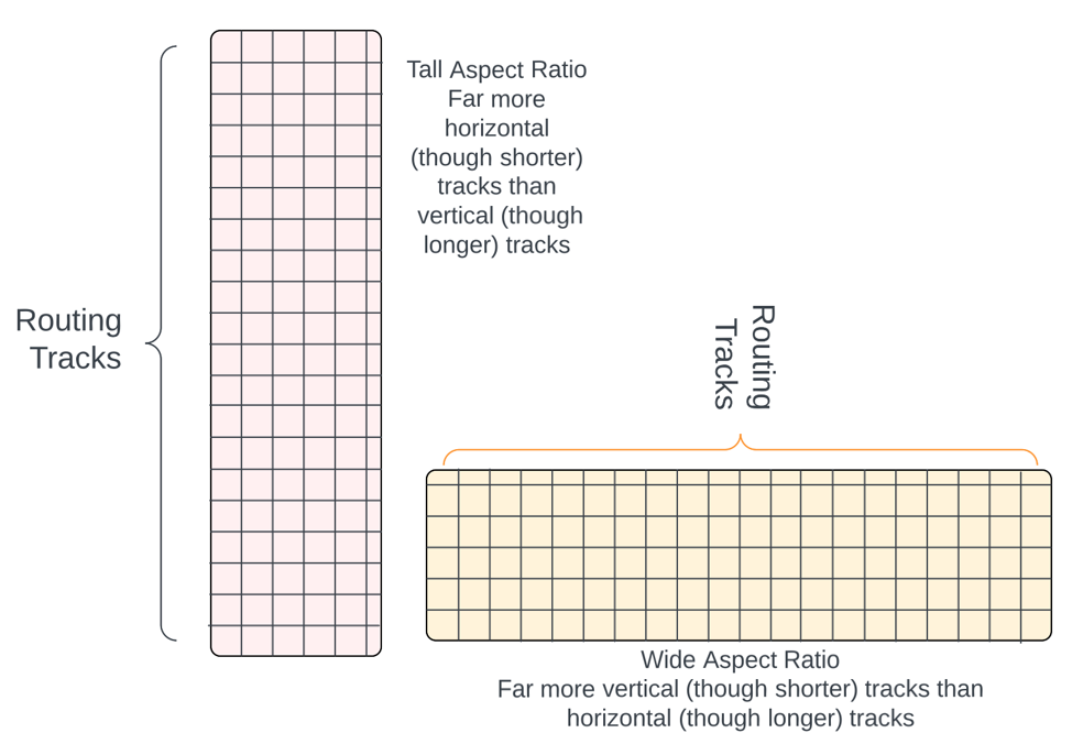
The aspect ratio of the floorplan refers to the ratio of block’s width to its height. It plays a significant role in the overall physical design of a chip as it impacts some key metrics that SoC designers need to be mindful of:
Routing Resources: A floorplan with a skewed aspect ratio has uneven routing resources in the horizontal/vertical direction. A taller floorplan has more horizontal tracks for routing, while fewer (though longer) tracks available for vertical routing. Similarly, a wider floorplan has fewer horizontal tracks available. Though top-level floorplan constraints might necessitate have a skewed aspect ratio for the floorplan, designers need to be mindful of these factors and try to mitigate it by opting for a smarter I/O pin placement or macro placement, if possible.
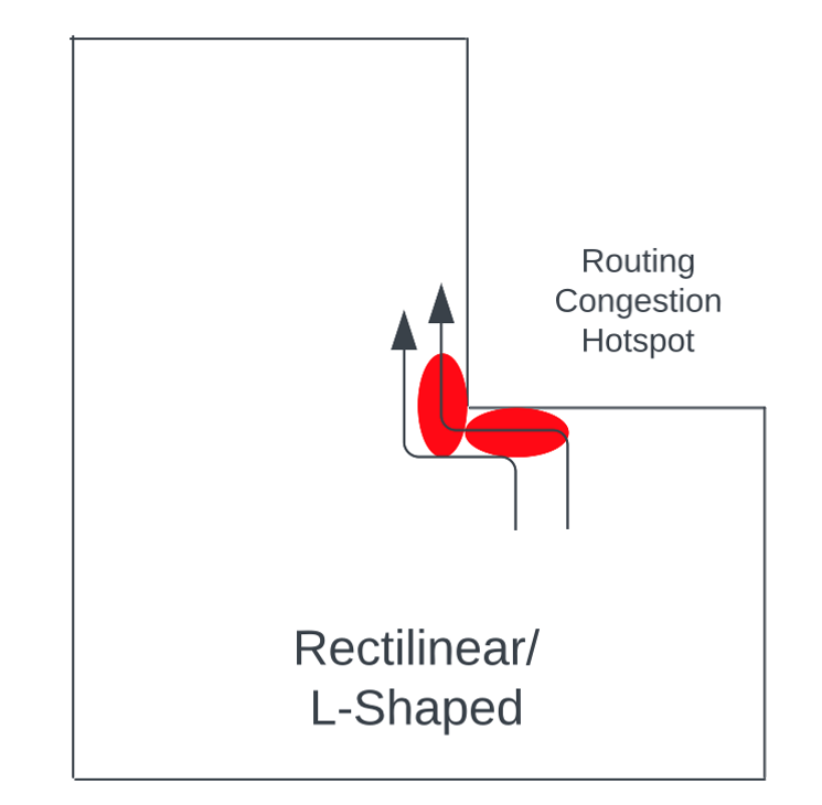
Routing Congestion around floorplan notches: For L-shaped floorplan, there may be a lot of wire traffic trying to cross the notch and these notches are usually susceptible to DRC blow up. By adding partial placement blockages or density screens, such issues can be avoided.
Now that we have a good idea of the trade-offs involved with different aspect ratios of the floorplan, designers would now need to define the floorplan and get started. But how big should the floorplan be? Coming up with the right floorplan size tends to be iterative while keeping in mind several factors:
Area Utilization: Area utilization is the fraction of total standard cell area over the total placeable area. If the floorplan is too small, the implementation tool will run out of placeable area during optimization and bail out fatally. On the flip side, if the floorplan is too big, that might result in the insertion of repeaters and may impact timing. It is therefore essential to hit the sweet spot with respect to overall area, timing, and power.
Routing Congestion: Even if there might be sufficient placeable area in each floorplan, a floorplan with very high utilization might be starved for routing resources and may result in routing DRCs due to pin accessibility issues or routing congestion.
Depending on the design, designers typically aim for 65-75% area utilization.
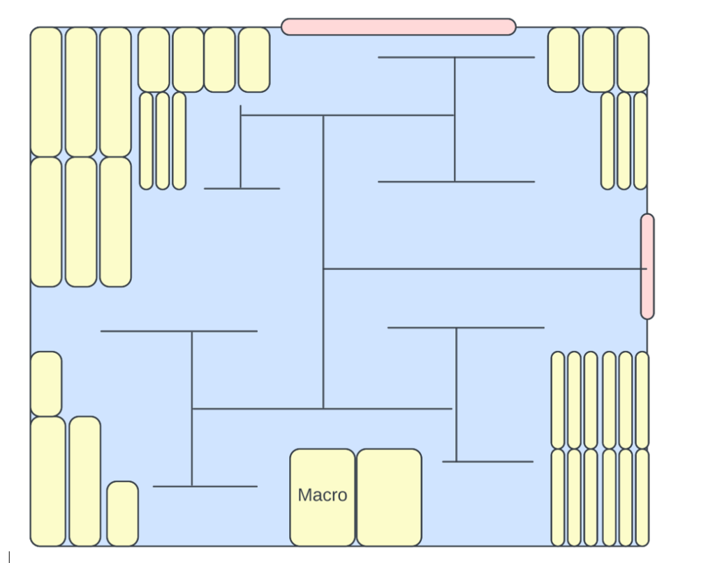
Hard macros are pre-designed blocks of logic or memory or intellectual property (IP) that can be integrated into a larger block or a chip. There are quite a few design considerations and trade-offs that designers need to balance while placing macros during the floorplanning step. We will discuss some of those factors here:
Macro Placement Strategy: Hard macros are typically stacked along the edge of the design coherent with the module placement in a manner such that:
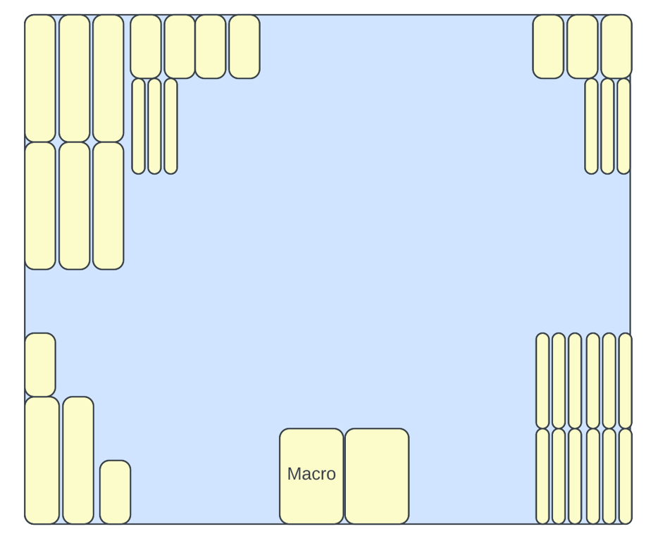
Channels between the macros: The narrow channels between the macros need special attention.
Signal Integrity and Crosstalk: Some macros could be analog design blocks like the SRAMs or other specialized IPs. Analog macros are more susceptible to noise and having a keep-out margin around the analog macros helps minimize the coupling between the adjacent signals and mitigate the deleterious effects of crosstalk noise.
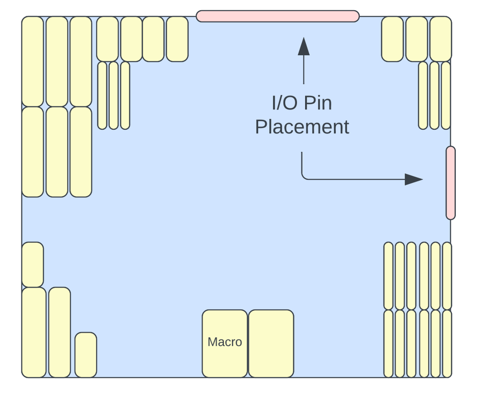
Placing the I/O pins is another key floorplanning activity that needs to be well planned. It refers to placing all the input and output pins along the edge of the block that act as the interface with the neighboring tiles. Designers try to place the pins with an aim to minimize the overall interconnect length, the routing and placement congestion near the interface. Following are some of the ideas to keep in mind while placing the pins:
Avoid Criss Crossing: In addition to connecting to the outside world, the I/O pins also connect to the internal logic. Designers must place the I/O pins while being cognizant of the internal logic modules that the respective pins interact with and their placement. They must avoid crisscross communication as it can result in routing congestion and blow up the routing DRC count.
Separate Layers: Designers should choose more than one layer while placing the pins and maintain sufficient spacing between the adjacent pins to avoid seeing shorts or other routing DRCs on the signals connecting to the I/O pins.
Physical Span: Physical span of the I/O pins should neither be too wide as it will cause the respective logic to spread and may result in timing issues nor can it be too narrow because that may cause the standard cells to be placed quite close to each other, thereby resulting in routing DRCs or may cause voltage drop hotspots near the ports.
Power Routing refers to the design of a robust delivery of power and ground signals throughout the chip. Drawing power wires and insertion of power switches are usually done at the floorplan step. Designers should carefully weigh the below trade-offs while designing a power grid for their chips:
Routing Resources vs Power Drop: While a strong power grid is in everyone’s best interests, it is not practical because a denser power grid limits the available tracks for signal routes. A sparse power grid will result in voltage drop issues and might therefore comprise the reliability of the fabricated chip.
Power EM: Power grid wires are susceptible to failing electromigration due to unidirectional flow of current through them. It is essential to create a mesh for power delivery to limit the current flowing through any net segment.
Standard Cell Placeability: The interactions of the power grid with the internal blockages or pins of the standard cells can limit the number of legal locations for placement. Designers must check the standard cell placeability score and adjust the power grid accordingly.
Designers should plan for the routing of their global signals like the clock or any other feedthrough signals in the floorplan step.
Clock: Designers should place the clock sources strategically to minimize clock skew and jitter. The clock distribution network must be carefully planned to ensure that the clock signals have a consistent and low-skew path to relevant clock domains
Feedthrough signals: Designers should allocate sufficient space for routing the feedthrough signals to avoid congestion and signal crosstalk. Plan the routing layers carefully such that the delay is minimize.
Signal integrity effects need to be carefully considered during the floorplanning step to ensure reliable signal propagation and minimize the signal integrity issues.
By identifying the critical signal paths, designers can prioritize their macro or pin placement to ensure a near-straight path for the critical signals, thereby minimizing the repeaters needed.
Shielding Analog signals: Analog signals are more susceptible to noise, and shielding these signals can help decouple them from neighboring signals and help preserve the signal integrity.
Electrostatic Discharge (ESD) Protection: Designers should add ESD clamp cells throughout the design to facilitate external noise affecting the internal circuitry. They need to plan for the placement for the bulky ESD clamps in the floorplan step to prevent any late disruption.
Thermal considerations are crucial in chip floorplanning to prevent overheating and to ensure proper heat dissipation. Overheating can degrade performance, reliability and shorten the lifespan of the chip. Some examples of thermal considerations are as follows:
Heat Sources: Some logical hierarchies like the execution unit of the Central Processing Units (CPUs) or the shader cores of the Graphics Processing Units (GPUs) are known to have high switching activity and tend to heat up more. Understanding these thermal constraints can guide the physical design engineers to determine an optimal placement location for these units.
Optimizing the Power Distribution: Ensuring a robust power delivery to the localized hotspots can reduce the overall dynamic voltage drop and minimize the frequency fall-out due to slowing down of standard cells.
Design for Manufacturability (DFM) rules have a significant impact on floorplanning as they influence the layout and arrangement of design components to ensure that the chip can be manufactured reliably and with high yield.
Metal Density Rules: DFM rules provide guidelines for the densities in each layer that need to be achieved to guarantee high yield. This can be achieved by using techniques like metal-fill to meet the constraint at the cost of high load capacitance observed by the signal routes.
Design Rule Check (DRC): DFM rules are typically enforced through Design Rule Checks during the physical design stage. These rules verify the adherence to DFM rules and identify any violations. Careful consideration of the DRC rules and checking initial feasibility can influence floorplanning decisions.
In conclusion, a well-executed floorplan is instrumental in achieving a correct-by-construction design for integrated circuits. By following the above ten essential floorplanning tips, physical design engineers can effectively manage complexity, optimize power distribution, address signal integrity issues, and achieve the desired performance, power, and area targets. Floorplanning needs iterative refinement and eventually culminates into successful chip layouts and improved design efficiency.


