

Wafer Level Packaging or WLP, is a type of IC packaging technology that is performed at wafer level. This means that the packaging is applied on whole wafers and wafers are diced only after the packaging is successfully competed. In wafer level packaging, the components used in assembly (such as bumps) are applied to the wafer pre-dicing, e.g. at wafer level. In traditional semiconductor manufacturing, the wafers are first diced into separate dies and then are assembled into a semiconductor package such as QFN or BGA.
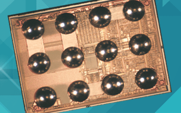
Figure 1: Wafer Level Packaging (image source: Amkor)
In addition to the small size and low cost benefits, Wafer-Level Packaging offers integration of wafer fabrication, testing, at the wafer level, resulting in a more streamlined manufacturing process, simplifying the journey a device undertakes from the silicon base to the finished shippable customer product.
Wafer-Level Packaging is also called Chip-Scale Packaging (CSP) and spilled into two main type of packages: fan-in and fan-out.
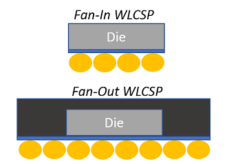
Figure 2: Fan in and Fan out pacakge types. Fan in (WLCSP) is essentially a bumped die
Before the advent of wafer level packaging, wires were used to connect the chips to the substrate, from the edges of the chip to the corresponding pins/pads on the substrate, in a process called wire-bonding. There are two main problems with wire-bonding: low electrical performance, hence do not fit to high performance and high frequency applications and limitation on the number wires per chip, thus creating a big barrier for the data transfer capacity of the chip in question.
As time progressed and Moore’s law made its effects more and more visible, circuits continued to be scaled down and shrunk, this made the wires thinner and longer, which created more problems, like wasted power and timing lag. This led to the inevitable transition to flip-chip packaging, which solved many of the dysfunctions caused by using wire-bonding. The flip-chip manufacturing technology consists of replacing the wires with solder bumps (referred to as pads or interconnect points) all over the top surface of the wafer, resulting in an increased density of electrical connections, from the area point of view. After dicing the wafer, the chips are flipped and attached to the substrate via bumped or copper pillars.
Wafer-Level Packaging, sometimes referred to as WLCSP (Wafer-Level Chip Scale Packaging), is currently the smallest available packaging technology in the market and is being offered by OSAT (Outsourced Semiconductor Assembly and Test) companies, like ASE, Amkor and others. A true WLP package though is formed from a wafer and an RDL (Redistribution Layer), interposer or I/O pitch, all of which serve the purpose of rearranging the pins/contacts of the die so that spread apart and big enough for better and easier handling.
Estimate NRE for test development and an indicative per-unit test cost.
Mainly, WLP can be split into two broad categories: Fan-In WLP (FIWLP or WLCSP) and Fan-Out WLP (FOWLP or eWLB). The difference between these two is at the interposer level. In the case of FIWLP, the interposer is the same size as the die, whereas in FOWLP packages the interposer is larger than the die, similar to conventional BGA packages.
What differentiates FOWLP and FIWLP from BGA packages is the fact that the interposer is applied directly on the wafer in the case of the WLP package, instead of making use of the flip-chip technique, where the BGA die is attached and reflowed to interposer. In both FIWLP and FOWLP packages, the die and the interposer can be encapsulated in a protective material, such as epoxy or thermo-resistant plastics.
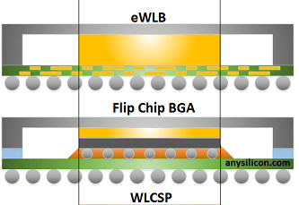
Figure 3: WLP vs BGA
FOWLP is a great alternative to TSVs (Through Silicon Vias) and it is beginning to gain popularity in the industry because it is a more economical way of achieving higher interconnect densities in compact spaces. This allows packages to become thinner and have a greater range of form factors.
The idea behind FOWLP is to reconstitute multiple/single chips onto an artificial wafer, which is made using low-cost polymers, and to ensure additional space is left between the chips for the interconnects. Then an RDL does a re-route of the connections from the chip to the peripheral areas. All in all, these techniques translate into a wider available range of form factors for the finished package and a much improved performance per watt when compared to a similar grid-array variant.
There are two primary FOWLP manufacturing processes:
One of the main uses for WLP was yet to come though, as I/O requirements kept growing and that demanded greater and greater interconnect density. This gave rise to the RDL (Redistribution Layer), which re-routes the connections of the chips via conductive metal traces.
RDL is also useful because it enables WLP packages to contain different chips with different functionalities, which became the System in Package, or SiP, for short. These encapsulated systems are frequently used in the mobile device market due to the fact that they can be made really compact to suit the space constraints and they also pack all the needed functionality into a single structure.
Another benefit of using the WLP methodology is the ability to stack chips vertically and/or tile them horizontally. This resulted in the development of 2.5D and 3D ICs, which make use of FOWLP technology and/or TSVs to connect multiple layers of dense horizontal interconnects (which are made out of copper) and ensure more bandwidth with less power consumption.
When using only TSVs, we say that the ICs use 2.5D spatial arrangements during manufacturing and are called 2.5D ICs for short. When we add multiple chips and stack them one on top of the other, we need to connect them with bumps and/or RDL (if needed), which creates an intricate 3D structure, thus the naming of such ICs as 3D ICs.
This new technology is being used in the server space, image sensors, gaming consoles, high-end supercomputing, artificial intelligence, and IoT (Internet of Things) devices. As the industry has not standardized the WLP methodology, there are a variety of different available schemes which can be considered. The decision comes down to the specific importance that device manufacturers impose upon reliability, cost, power consumption, performance and even form factor.
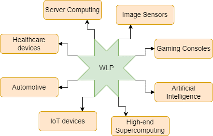
Figure 4: Sectors where Wafer-Level Packaging is relevant
One of the major domains captured by Wafer-Level Packaging technologies in the smartphone sector. With the strenuous and ever increasing size constraints, mobile devices are the perfect application for WLP packages, seeing as the functions the WLPs provide range from sensors, cameras, wireless connectivity, and power management.
For example, there are at least eleven WLPs in an Apple iPhone 5, six WLPs in a Samsung Galaxy S3, and seven WLPs in an HTC One X. This makes it clear that WLPs are here to stay in the smartphone segment, but the same advantages that got it to the top of this segment is also propelling it to the top of many others: IoT devices, automotive chips, healthcare devices, artificial intelligence machines, and many more.
As for the economics of Wafer-Level Packaging technology, in 2020, the global wafer level packaging market size was $3.61 billion and the investor expectation is that it will reach $7.672 billion by the end of 2027, with a CAGR (Compound Annual Growth Rate) of 10.9% between 2021 and 2027.


