

Abstract
Expanding its ChipArray® Ball Grid Array (CABGA) package form factor miniaturization efforts, Amkor now offers a maximum 0.40 mm height CABGA assembly process. Amkor’s latest CABGA process has been extensively demonstrated, evaluated and optimized to provide reliable, high-quality production. By extending CABGA capabilities to various competing near die size packaging options, customers can obtain the benefits of this low-cost packaging alternative from an advanced, well-proven manufacturing process with widely available high-volume manufacturing (HVM) capacity while achieving high I/O integration. The new package addresses the requirement for ever continuing IC component size reduction in the electronics industry. From this study, wire bond CABGA has proven its capabilities and potential for continuously and effectively competing with existing and emerging advanced packaging options.
Introduction
The wire-bond ChipArray® Ball Grid Array or CABGA package is a very popular packaging option. The CABGA package provides versatile solutions for a broad array of semiconductor products used in a variety of automotive, industrial, computing, networking, consumer and mobile applications. In addition to offering high performance and flexible signal routing capability for high I/O count devices, the CABGA’s small footprints and thin form factors make it a member of the so-called near die size packaging category for single-die products in the semiconductor industry. Continuously expanding capabilities in mobile handsets has always required a continuous reduction in all semiconductor components form factor, both footprint and height. To keep up with the industry’s size reduction pace, the wire bond CABGA packaging process has faced many issues in key process areas. Amkor has successfully and continuously developed advancements to address these challenges.
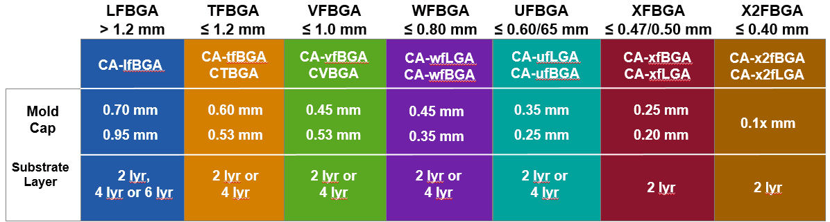
This paper introduces and reviews Amkor’s latest achievement of developing a maximum 0.4 mm height fine-pitch ball grid array (FBGA), called X2FBGA (Table 1) to denote a double extreme thin FBGA form factor. It discusses key challenges and actions taken to make the assembly process feasible and bring solutions to market. It will also review the X2FBGA’s advantages and potential position among the various near die size packaging options available in the market, such as the Quad Flat No-Lead (QFN) package, routable QFN package, flip chip chip scale packaging (fcCSP) and wafer-level packages.
Table 1) Amkor’s ChipArray BGA offerings: low-profile fine-pitch BGA (LFBGA), thin-profile fine-pitch BGA (TFBGA), very fine-pitch BGA (VFBGA), very very thin-profile fine-pitch BGA (WFBGA), ultra-fine BGA (UFBGA), extremely-thin fine-pitch BGA (XFBGA), and X2FBGA
Background/Problem Statement
In recent years, advanced package options are very diversified in terms of form factors, substrate technology and the enabling process technology (see Figure 1). For single-chip packaging, the QFN package has achieved large market share among leadframe-based packages as a fast-growing option. QFN evolution extended its multi-row I/O capabilities in peripheral land construction that is similar to designs of area-array I/O of the laminate substrate FBGA package. More recently, QFN packaging has further advanced by offering internal trace routing solutions using a pre-molded routable leadframe or a molded interconnect substrate.
On the wafer level packaging (WLP) side, Fan-in WLP (also known as die size BGA or DSBGA) has established another mainstream branch of the advanced package family providing true die-size packaging. The fcCSP uses exactly the same package outline platform as the wire bond CABGA and it enables more complicated interconnecting options and higher I/O count with high efficiency and superior electrical performance.
Today, all of the above packages can achieve a total seat profile less than 0.4 mm. The Fan-in WLP height is determined by the wafer backgrind thickness during the backend process, so it is relatively easy to achieve. For QFN package’s mold cap tooling determines the body profile. With 0.25 mm mold cap tooling, which has been commonly used for several years, only the leadframe thickness needs to be included. The fcCSP has the option to expose the die backside on top of package, so its thinness control is a relatively easy way to offer a maximum 0.4 mm profile.
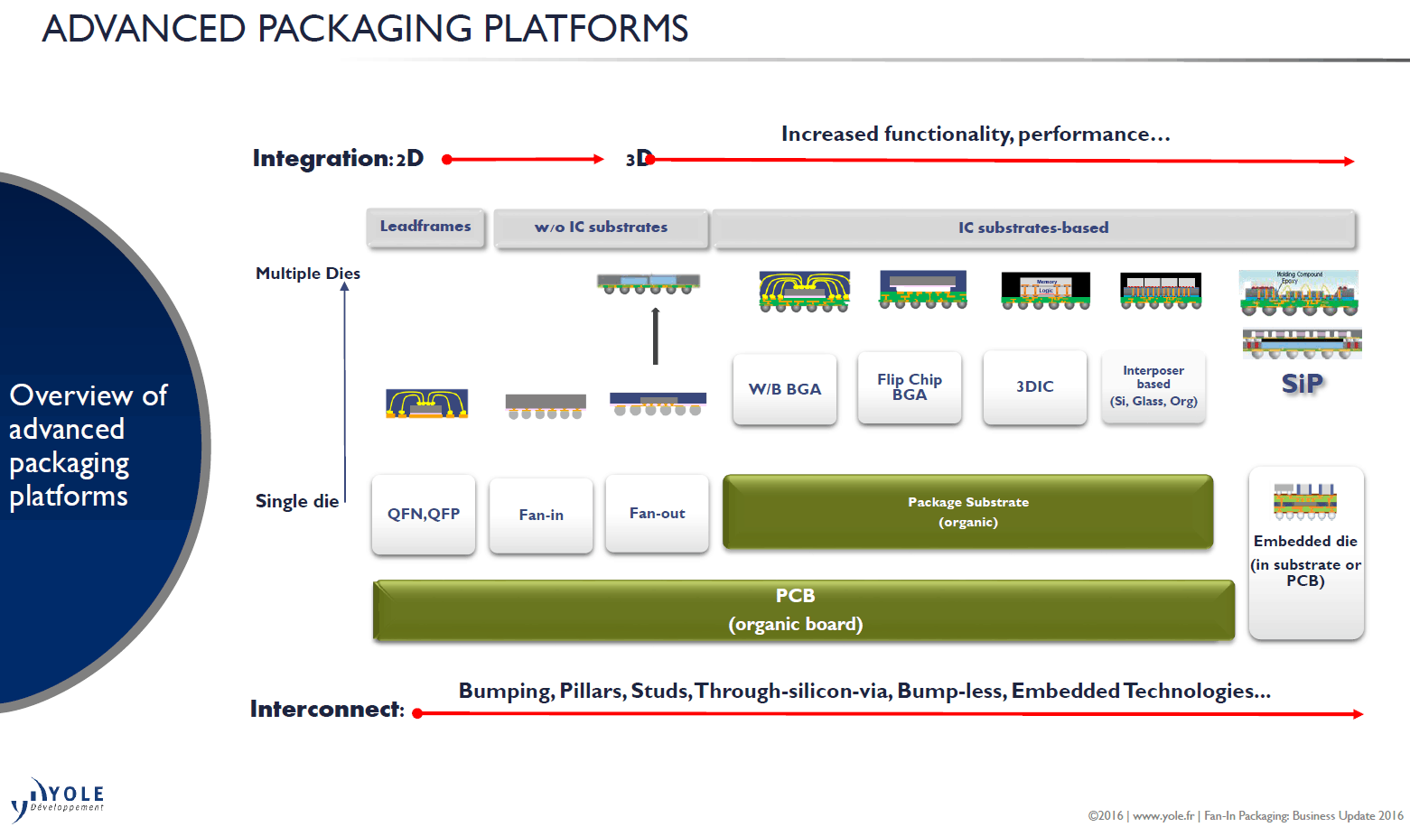
Figure 1) Evolution of advanced packaging. Courtesy of Yole Développement.
Compared to other packages, wire bond CABGA has more challenges to achieve a thin package profile. The added height of the CABGA solder ball bumps requires thinner die and ultra-low wire looping controls to fit all z-dimension stack-up elements within the thin mold cap space. The extremely-thin fine-pitched BGA (XFBGA) provides a maximum 0.47 mm (or 0.50 mm) height physical profile dimension, and, until recently, it has been the thinnest wire bond BGA achievable using traditional face-up die bond, wire connect and molding process technology combined with a commonly available thin 2-layer laminate substrate. Based on XFBGA thickness reduction, CABGA’s miniaturization capability, approaching the IC die size, has been improved by tighter control of die edge to bond ring and the tighter clearance control of die-to-package body edge. This extended miniaturization capability is essential for the wire bond CABGA package to expand its applications in various market sectors especially in mobile devices.
As discussed previously, other advanced packaging options continue to address the need for ever thinner packages. In many cases, the same advancements are required to reduce wire bond CABGA components’ form factor. As all the packages continue to improve, there are still many advantages that the wire bond CABGA provides for specific applications – if it meets the form factor requirements.
With its signal routing flexibility and dense I/O integration capability, the wire bond CABGA design is superior to QFNs. Compared to Fan-in WLP, the wire bond CABGA also maintains comparable I/O capability, since the DSBGA I/O number is limited by its own die size. Reducing its ball pitch to integrate more I/O, the DSBGA tradeoffs include SMT quality and yield control issues for finer bump pitch. Flip chip CSP design can overcome these technical issues and provide another effective solution, but it requires a bumping process on the die, which is a major cost addition, especially if the die design does not allow users to enable cheap enough bumping and under-fill methods. In many instances, wire bond CABGA packaging is an attractive solution.
More recently, the fan-out wafer level package (FO-WLP) has garnered a lot of attention by creating a new paradigm of semiconductor integration capability using reconstituted wafer level technology that employs a redistribution layer (RDL) process or even the panel level RDL process. For two or more die (multi-chip) integration, the FO-WLP, using an RDL process with or without interposers plus the package stack, is attracting major interest for applications that require high speed and high bandwidth performance such as mobile application processors.
In contrast, the application of the single die FO-WLP is still being decided in terms of die/package size sweet spot area, although it’s clearly shown its continuing growth trajectory for some time. The same situation may exist for some of the relatively simple two to three die integration achievable with wire bond, since there are many existing packaging solutions with process technology and form factor advantages that are low cost and have high volume capacity. For applications where the I/O density requires the package to be larger than the die, CABGA and FO-WLP can be considered. FO-WLP has advantages with regards to ultra-thin packages, and the CABGA format is very cost competitive. Introducing the CABGA at a thickness near the FO-WLP limit, would provide a compelling option for those wanting the best attributes of both. Table 2 shows packaging options with maximum I/O and maximum profile thickness capabilities. The 2~7 mm body size range could be the sweet spot of the market opportunity that wire bond CABGA packages can contribute considering today’s die size and I/O number trend.
Taking these factors into account, wire bond CABGA packaging is expected to have significant acceptance and contribute to further growth in this market with continued miniaturization in the near die size packaging field. To achieve a near-term product, the maximum 0.40 mm profile wire bond CABGA process capability was targeted. The main technical challenges in this development occur in four key areas: design, material, process and method.
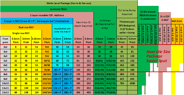
Table 2) Near die size packaging I/O density options and sweet spot analysis.
Solution
Designing the cross-sectional structure and its geometrical details as well as setting control limits during substrate manufacturing and IC assembly processes are the foundations for successfully building the X2FBGA. These areas establish the goals of each process and provide the targets to reach. To achieve the final maximum 0.40 mm BGA height including tolerance limit, the nominal z-height dimension must be reduced; 0.35 mm was set as a final nominal dimension target to allow a +0.05 mm tolerance specification limit. Compared to the existing XFBGA (see Figure 2), this required 28% tightening of overall tolerance in addition to a 12.5% reduction of actual packaging material thickness. Mold tool design, substrate tolerance, and the associated design features to control bump ball height are all required to adjust, tighten and meet the target thickness reduction.
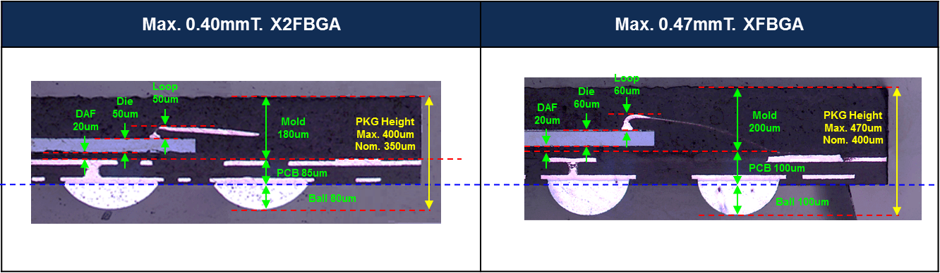
Figure 2) Cross-sectional comparison of the XFBGA and X2FBGA packages construction.
Material selection for mechanical property management is another challenge. The substrate core and solder mask material selection must be stiff enough to withstand and maintain the flatness of the substrate throughout the assembly process. Lower coefficient of thermal expansion (CTE) and ultra-thin (40-µm) core material combined with a low-CTE solder mask is required to control the deflection and deformation of the raw PCB substrate and after bake die attach (D/A). See Figure 3.
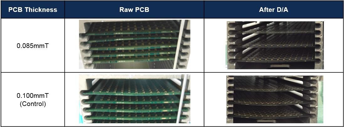
Figure 3) Substrate in the front end of line (FEOL) process magazine, showing deflections and warpage management.
The mold compound’s physical properties were studied and chosen to prevent the molded strip warpage and maintain high quality and productivity during the backend of the assembly process.
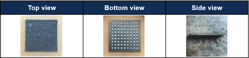
Figure 4) X2FBGA picture after finishing assembly
Wafer thinning and strength management, including sawing methods, are also important.
The 50 µm wafer thickness and die handling are performed to prepare for subsequent assembly processes. With this construction, the die top to mold cap leaves a z-space of only about 110 µm. In addition to the ultra-low wire looping control at wire bond process, the review and control procedure of the markable area on the body top surface must be considered during production planning to prevent potential interaction of the laser mark engraving depth with wires. Figure 4 shows the end results.
A micro solder ball formation process with 80 µm or less bump height has been in HVM for many years. Its production capabilities and market acceptance are well established for WFBGA and UFBGA packages. However, in some applications, customers specify a nominal 100 µm bump height as the de facto application requirement. To prepare for and address such an application requirement, an additional 10-20 µm of tooling reduction and adjustment in mold tool and die thickness have also been provided to allow additional bump space in the final package.
To certify its volume production readiness level, the X2FBGA package has been submitted through an internal qualification procedure and reliability tests. With all testing completed, the X2FBGA package passed all qualification requirements. Since this package targets mobile device applications, a conformal electromagnetic interference (EMI) shielding process is offered as an option. The BGA form adds challenges in shield coating since the ball bumps require masking to prevent coating material contamination on the bottom side. As a result of targeted efforts in process development for a micro bump BGA conformal shield, Amkor now offers a shield process up to a 100-µm bump height BGA. See Figure 5.
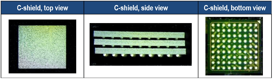
Figure 5) X2FBGA after conformal shielding
Conclusion
Amkor has extensively studied where and how the wire bond CABGA can increase its offerings of advanced miniaturized packaging solutions. As a result, design, process, bill of material (BOM) and method advancements have been developed and implemented into Amkor’s manufacturing processes to offer the X2FBGA package’s capabilities. Ultra-thin substrate design, sourcing, the right assembly material selection, tooling and process combinations are all available to support a variety of customer needs. Customers are now encouraged to consider the X2FBGA (with other advanced packaging options based on pros and cons) for their IC packaging needs and take advantage of its capabilities to satisfy existing and emerging design requirements.
For More Information
For more information, please contact burt.barber@amkor.com or yeonho.choi@amkor.com
ChipArray is a registered trademark of Amkor Technology, Inc.
© 2017 Amkor Technology, Inc. All Rights Reserved.


