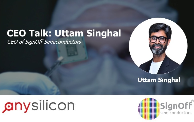
This interview features: Uttam Singhal, CEO, SignOff Semiconductors Pvt. Ltd.
Tell me a bit about your background? How did you first get started with your company?
I have spent over 25 years in the semiconductor industry, beginning my career in full-custom analog and memory design before transitioning into large-scale SoC physical design. Over this journey, I have had the privilege of working with leading organizations such as STMicroelectronics, AMD, and Intel, contributing to numerous complex tape-outs across a wide range of process nodes – from mature technologies to the most advanced nodes.
I joined SignOff Semiconductors in its early days, when the company was still a very small, tightly knit team with big ambitions. What began as an advisory and business leadership role quickly evolved into a fulltime commitment as I saw the passion, agility and technical depth in the group and wanted to help shape it into a global design services organization.
Tell me about SignOff Semiconductors.
SignOff Semiconductors is a design services company focused on end-to-end ASIC and SoC development, with deep expertise‑ in physical design, verification, RTL design, Design for‑ ‑Test (DFT), Full-custom layout‑ and Embedded solutions. We like to describe ourselves as an engineering-first organization: our reputation rests on the quality of our ‑tapeouts‑ and the way we collaborate with customer teams.
We are headquartered in Bengaluru, with additional presence in Hyderabad, Toronto, California, Malaysia and Israel, which allows us to support customers across India, North America and key global design hubs in compatible time zones. Our customers range from fast-growing fabless startups to established semiconductor leaders in markets like automotive, mobile, datacenter, and IoT.
When did you start SignOff Semiconductors? What were you doing before that?
SignOff Semiconductors was founded in 2015 by a group of experienced semiconductor professionals who wanted to create a focused, high-quality design services partner. Before joining SignOff, I led globally distributed teams across multiple geographies while owning end-to-end SoC delivery at large product companies, working on discrete graphics and machine learning chips and taking them through full signoff and tapeout.
What attracted me to SignOff was the combination of strong technical depth and a very transparent, people centric culture. It felt like the right place to bring my experience in both engineering and leadership and help build something long-term.
What problem did you see that needed to be fixed? What is your approach to solving that?
The main gap we saw was that many companies struggled to find flexible, high-caliber design teams that could reliably own critical blocks and subsystems through to signoff. Having a design partner who can take ownership and be accountable of contributing towards a competitive solution was the industry’s aspirational expectation. In most existing solution providers, either the expertise was too narrow, or the engagement model was too rigid for fastmoving programs.
Our approach has been to build strong inhouse expertise across the full flow from RTL and verification through physical implementation, full custom layout and signoff and then engage in a very transparent way. We behave like an extension of the customer’s team: same goals, same urgency, clear communication and a strong sense of ownership for first time right silicon.
How has the role/offering of SignOff Semiconductors changed in recent years?
We started primarily as a physical design and full‑custom layout partner and, over time, expanded into broader digital design, verification, design‑for‑test (DFT) and embedded engineering. This shift was driven by customers who wanted fewer hand‑offs and more accountability from a single partner.
In parallel, we have moved from being purely a resource augmentation vendor to deeper engineering contribution while taking on more turnkey responsibilities, including owning complete blocks and subsystems. Acting as a primary implementation partner alongside the customer’s fullchip team is always the end goal for us. That naturally pushed us to invest more in methodology, IP integration expertise, and leadership bandwidth.
Which market segment seems most promising to you, and why?
We continue to see strong demand in automotive, high-performance compute, memory design , and connectivity-driven IoT applications. These segments typically need either advanced process nodes, complex power performance tradeoffs, execution excellence, and long product lifecycles, which play well to our strengths in signoff driven design.
Another area we find interesting is the intersection of AI and edge devices, where customers want to squeeze a lot of intelligence into very tight power and cost budgets. The introduction of generative AI models for faster execution is game-changing. For an engineering-driven services company, these are exactly the kind of problems that keep the team motivated.
What is a typical customer for SignOff Semiconductors?
A typical customer for us is a fabless or systems company with an active or upcoming ASIC/SoC program which needs additional, experienced hands to close it on time with predictable quality. They usually have strong internal architects and product owners, and they look to us to bring deep implementation expertise, strong workflow expertise, and stable engineering capacity for their key blocks and subsystems.
We work with both large, well-known semiconductor companies and smaller, fast-growing startups that may be doing their first or second chip. In both cases, what they value is a partner who can ramp quickly, communicate clearly, and stand behind the tapeout.
Customers are focused on time-to-market, first-time-right, price, etc. Do you see a change in customer behavior in recent years? Where is the focus today and why?
In the last few years, we have seen customers become much more sensitive to schedule risk and predictability, especially as nodes get more advanced and mask costs increase. First-time-right has always been important, but now it is almost nonnegotiable.
At the same time, there is more emphasis on building longer-term engineering partnerships rather than just executing a single project at the lowest possible cost. Customers realize that stable teams and good retention at the services partner are key to maintaining quality across multiple generations of their products.
As a service company we are also adapting and getting our engineers upgraded to AI model adoption sooner than later to differentiate and reflect value add in making time to market and lower cost a reality.
Are you currently hiring? What type of jobs?
Yes, we are continuously looking for engineers who enjoy working on challenging chips and want to grow with a services company that values depth of expertise. The jobs vary across RTL design, verification, physical design, full-custom layout, and related signoff areas, at both junior and senior levels.
We are always looking for strong technical leadership role fulfilment where people can drive complete blocks or programs and mentor younger engineers. Openings are typically listed on our careers page, and we are always happy to hear from strong candidates and leaders, even if a specific role is not posted yet.
What is your #1 advice for people who want to work for your company?
My main advice is to be curious and be ready to take ownership. In a services environment, you are exposed to a variety of designs, customers, and flows, which is a great opportunity if you are willing to constantly learn.
A strong work ethic, respecting your team members and a genuine interest in solving difficult engineering problems as a team will take you a long way. If an engineer brings that mindset, the company will invest in their growth.
Where can one find more information?
The best starting point is our website, where you can learn more about our domains, services, and current openings. We also share updates and insights on our LinkedIn page and through industry platforms like AnySilicon.
For specific project enquiries, there is a contact form on our site, and our team is quite responsive over email. We are always open to exploratory conversations, even if your next tapeout is still some distance away.
What is the best moment in your day?
The best moment for me is whenever I am talking to our engineers about a tough problem they just solved or a milestone they have reached. Seeing their enthusiasm and pride while sharing their success story reminds me why we are building this company.
I also enjoy customer feedback where we receive appreciations and updates about their silicon results from past tapeout projects. There is something extremely satisfying about seeing months of collective effort turn into a working chip.
How do you keep yourself energized and engaged during the day?
I like to keep myself engaged with the latest technological buzz, industry trends, and talks about incoming challenges. I also like to alternate between deep work thinking about technological trends, and organization building that would be ready to cater to the forthcoming demands. That balance between having discussions with my engineering teams over their ongoing projects and keeping a close watch on industry trends keeps me connected to both the long-term vision and the day-to-day realities.
Whenever possible, I also try to step away from the screen for short walks or casual conversations with colleagues; some of the best ideas and decisions happen in those informal settings.


