




Advanced Semiconductor Engineering, better known as ASE, has announced the development of an automated 310mm × 310mm panel-level packaging production line. The move is another sign that advanced packaging is becoming a critical part of semiconductor scaling, especially for AI processors, high-performance computing devices and chiplet-based architectures.
For years, the semiconductor industry relied mainly on wafer-level packaging and traditional substrate-based approaches. But as large AI accelerators and multi-die systems become more complex, packaging is no longer just a back-end assembly step. It is now a central part of system performance, cost, yield and supply-chain strategy.
ASE’s new panel-level packaging line is designed to improve manufacturing efficiency by moving from round wafer formats to rectangular panels. A 310mm × 310mm panel provides up to 96,100 mm² of usable surface area, creating opportunities for better material utilization and higher package output per manufacturing cycle.
Panel-level packaging, or PLP, is an advanced semiconductor packaging approach in which chips are processed on a rectangular panel instead of a circular wafer. The basic idea is similar to wafer-level packaging, but the larger panel format can provide more usable area and potentially lower cost per package when the process is mature.
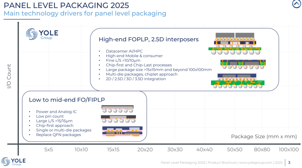
In fan-out panel-level packaging, known as FOPLP, dies are placed on a carrier panel and embedded in mold compound. Redistribution layers are then built to route signals from the die to a larger package footprint. This allows the package to support more I/O, better electrical routing and thinner form factors.
The main advantage of panel-level packaging is scalability. A rectangular panel can reduce wasted edge area compared with a round wafer and can support higher package counts per panel. This is especially attractive for applications where advanced packaging volume is increasing quickly.
However, panel-level packaging is technically challenging. Larger panels are more difficult to control during processing. Warpage, die shift, alignment accuracy, redistribution layer quality and yield control all become major issues. For this reason, automation and process control are essential for bringing panel-level packaging into high-volume production.
ASE’s new automated line supports a 310mm × 310mm panel format. According to ASE, the line is compatible with its advanced packaging platforms, including FOCoS and FOCoS-Bridge.
FOCoS, which stands for Fan-Out Chip-on-Substrate, is ASE’s fan-out packaging platform for high-performance applications. In this approach, fan-out technology is combined with a substrate to support high pin counts, improved routing and integration of multiple dies.
FOCoS-Bridge uses small silicon bridge structures inside the package to connect chiplets. This type of approach is increasingly important as the industry moves from large monolithic chips toward multi-die designs. Instead of building one very large die, companies can combine multiple smaller dies, or chiplets, inside one advanced package.
ASE says the new line supports line/space capabilities of 2/2µm for FOCoS and 8/8µm for FOCoS-Bridge. These dimensions are important because fine line/space routing enables higher interconnect density between dies, memory and substrates.
AI processors are pushing packaging technology to its limits. Modern AI accelerators often require large logic dies, high-bandwidth memory, wide I/O interfaces, advanced thermal management and very high interconnect density.
Traditional packaging methods are not always sufficient for these requirements. As AI systems become more powerful, the package must support faster communication between compute dies and memory, lower power loss and higher bandwidth.
This is one reason why advanced packaging has become a competitive battleground. TSMC, Intel, Samsung, ASE, Amkor and other companies are investing heavily in technologies such as 2.5D packaging, fan-out, silicon bridges, interposers and chiplet integration.
ASE’s panel-level packaging announcement fits directly into this trend. By using a larger panel format, ASE aims to improve manufacturing scalability and efficiency for advanced packages used in AI and HPC applications.
Wafer-level packaging has already become important in smartphones, automotive electronics, RF devices and certain high-performance applications. But wafer formats create natural limitations because round wafers do not use all available manufacturing area efficiently.
Panel-level packaging attempts to address this by processing packages on rectangular panels. This is conceptually similar to how the display and PCB industries process large rectangular substrates.
The potential benefits include:
The challenge is that semiconductor packaging requires much tighter tolerances than many traditional panel-based manufacturing processes. For advanced AI packages, even very small alignment errors can affect yield and performance.
That is why ASE’s focus on automation is important. Automated handling, placement, inspection and process control are required to make panel-level packaging practical for high-end devices.
ASE’s FOCoS platform is designed for high-performance fan-out applications. It combines fan-out redistribution with a package substrate, making it suitable for large, high-I/O devices.
In a typical fan-out structure, the die is embedded in mold compound and redistribution layers are used to route connections outward from the die. This allows the package to support more external connections than the die surface alone would allow.
FOCoS-Bridge adds another layer of integration by using silicon bridge technology. A silicon bridge can provide dense, short interconnects between chiplets inside the package. This can be more cost-effective than using a full silicon interposer in some applications, while still enabling high-bandwidth die-to-die communication.
This type of architecture is especially relevant for chiplet-based AI accelerators, where logic, memory interfaces and other functions may be separated into different dies and then integrated inside one package.
ASE is the world’s largest outsourced semiconductor assembly and test company, and its move into automated panel-level packaging highlights how important OSATs have become in advanced semiconductor manufacturing.
Historically, foundries received much of the attention in semiconductor scaling. But today, packaging companies play a much larger role in enabling system-level performance. Advanced packaging can determine whether a chip can meet bandwidth, power, thermal and form-factor requirements.
For fabless semiconductor companies, this creates new decisions during product planning. Packaging choices must now be considered much earlier in the design cycle. The package architecture can affect die partitioning, I/O planning, thermal design, substrate selection, test strategy and total cost.
As AI and chiplet designs grow, the relationship between foundries, OSATs, substrate suppliers, EDA vendors and system companies becomes more tightly connected.
Although panel-level packaging offers major advantages, it is not a simple replacement for wafer-level packaging. Several technical challenges must be managed carefully.
One major issue is warpage. Large molded panels can bend or deform during thermal processing. Warpage can affect lithography, alignment, assembly and yield.
Another issue is die shift. During molding and processing, embedded dies can move slightly from their intended positions. In packages with fine redistribution layers, even small die movement can create alignment problems.
Inspection is also more complex. Large panels require accurate metrology across a bigger area. Any process non-uniformity can impact yield.
Finally, supply-chain readiness is important. Equipment, materials, substrates and process flows must all support panel-based manufacturing at high volume. This requires coordination across the packaging ecosystem.
For fabless semiconductor companies developing AI, HPC, networking or advanced automotive chips, ASE’s panel-level packaging line is important because it expands the available packaging options.
Companies planning chiplet-based products must evaluate packaging early. The decision between fan-out, 2.5D interposer, silicon bridge, organic substrate or panel-level packaging can significantly affect cost, performance and manufacturability.
Key questions include:
Panel-level packaging may become attractive when the package requires high integration density and high-volume manufacturability, but does not necessarily need the most expensive full-interposer approach.
The launch of ASE’s 310mm × 310mm panel-level packaging line shows that advanced packaging continues to move from a niche technology into a mainstream scaling path.
As transistor scaling becomes more expensive, the industry is using packaging to improve system performance. Instead of relying only on smaller process nodes, companies are combining multiple dies, specialized chiplets, advanced substrates and high-density interconnects.
This shift is changing the semiconductor value chain. Foundry selection is still critical, but packaging strategy is now just as important for many high-end products.
ASE’s announcement is therefore more than a packaging update. It is another sign that AI chip manufacturing is increasingly dependent on advanced assembly, high-density interconnect and scalable packaging platforms.
ASE’s automated 310mm × 310mm panel-level packaging line represents an important step in the evolution of advanced semiconductor packaging. By supporting FOCoS and FOCoS-Bridge platforms, ASE is targeting some of the fastest-growing areas in the semiconductor market: AI, HPC and chiplet-based system integration.
Panel-level packaging offers the potential for better material utilization, higher manufacturing efficiency and improved scalability. At the same time, it requires strong process control, automation and advanced materials expertise.
For semiconductor companies developing next-generation AI and chiplet products, packaging is no longer a final step after silicon design. It is a core architectural decision that can shape performance, cost and time-to-market.
As advanced packaging capacity becomes increasingly strategic, ASE’s move strengthens its position in one of the most important parts of the semiconductor supply chain.
AnySilicon helps semiconductor companies connect with trusted ASIC design, foundry, packaging, assembly and test partners. If you are planning a chip project and need support with package selection, OSAT sourcing, ASIC manufacturing or supply-chain planning, contact AnySilicon to discuss your project requirements.