


Custom ASIC Solutions: From Specification to Silicon
Developing a custom ASIC is one of the most important decisions a hardware company can make. A well-designed ASIC can reduce power consumption, improve performance, lower unit cost at volume, protect intellectual property, and create a product advantage that is difficult for competitors

Find Qualified Wafer Dicing Suppliers for Your Semiconductor Project
Wafer dicing is a critical step in semiconductor manufacturing, where processed wafers are separated into individual dies or chips before packaging, assembly, testing or further processing. The dicing process must be accurate, clean and well controlled, as poor dicing can lead
In the world of high-speed SoC design, “almost working” is really just a polite way of saying “an expensive paperweight.”
As we push beyond the 6.4 Gbps threshold with DDR5, the margin for error has essentially disappeared. For engineering leads and decision-makers, the goal is no longer just a

Developing high-performance analog ICs requires deep expertise, precise design methodologies, and strong understanding of process technologies. From power management and sensor interfaces to data converters and high-voltage applications, analog IC design is one of the most specialized areas in semiconductor development.
AnySilicon helps companies connect with experienced analog IC
Need Expert ASIC Design Support?
From concept definition to tape-out, ASIC development requires deep technical expertise, strong foundry relationships, and access to the right design resources. AnySilicon helps companies connect with trusted ASIC design consultants and experienced design houses for analog, mixed-signal, RF, digital, and full-custom IC development.
Read More
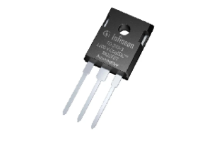
What is a TO-247 Package?
The TO-247 package is a widely used through-hole semiconductor package designed for high-power applications. It is commonly used for devices such as MOSFETs, IGBTs, diodes, and power transistors that require efficient heat dissipation and high current handling.
TO-247 stands for “Transistor Outline 247”, and