

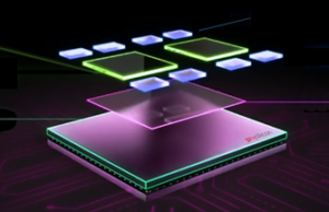
Advanced packaging has become the place where AI system performance is won or lost. High-end performance packaging revenue is forecast to grow to more than $51 billion in 2031, a 27% CAGR during 2025-2031, with package unit volume expanding at a 33% CAGR and wafer demand at 30%.
Read More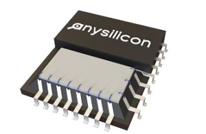
IC prototype packaging is the bridge between first silicon and a device that engineers can actually handle, mount on a PCB and evaluate. For most prototype ASICs, sensors, mixed-signal ICs and MPW shuttle dies, the best approach is to use an existing package platform such as QFN, QFP, BGA or
Read More
For semiconductor products entering production today, silicon remains the strongest choice when maximum routing density, proven HBM integration and the most demanding chiplet-to-chiplet bandwidth are required; organic or RDL interposers are usually more attractive when cost, large package size and mechanical compliance matter more than absolute interconnect density; and glass
Read More
The practical difference is simple: 2.5D packaging places multiple dies side-by-side and connects them through a high-density interposer or bridge, while 3D packaging stacks dies vertically and connects them through TSVs, microbumps or hybrid bonding. In 2026, 2.5D remains the mainstream architecture for large AI accelerators, GPUs and HBM-based systems
Read More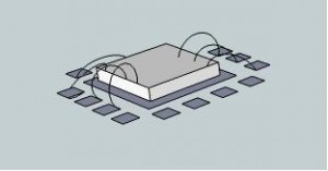
VQFN stands for Very Thin Quad Flat No-Lead, and it is best understood as a low-profile member of the QFN family rather than a fundamentally different package architecture. Like a standard QFN, a VQFN has no protruding gull-wing leads; the electrical terminals are located mainly on the bottom perimeter
Read More
QFN is usually the better choice when your priorities are minimum PCB area, short electrical paths, RF/high-frequency performance and efficient heat transfer into the PCB; QFP is usually the better choice when visible solder joints, easier optical inspection, probing and rework are more important. The fundamental difference is mechanical:
Read More