


Asia-Pacific’s grip as the dominant market for IC sales is forecast to strengthen in 2016 with the region expected to account for 61.0% of the $282.0 billion IC market this year, based on analysis published in IC Insights’ mid-year Update to the 2016 IC Market Drivers report.
Read More
Neuchatel, 11 October 2016 – CSEM, the Swiss Research and Technology Organization, today announced that they have licensed their IcyTRX™ silicon RF IP core to Danish hearing aid manufacturer Oticon.
Oticon has integrated IcyTRX™ IP core into their new chipset for the new Oticon Opn™ range of advanced wireless-enabled
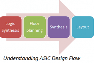
Today, ASIC design flow is a mature process with many individual steps. ASIC design flow process is the backbone of every ASIC design project. To ensure design success, one must have: a silicon-proven ASIC design flow, a good understanding of the ASIC specifications and requirements, and an absolute domination over
Read More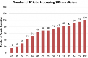
Enormous financial and technology hurdles continue to plague the development of 450mm wafers. Ambitious goals to put 450mm wafers to use have been scaled back. IC manufacturers are instead maximizing their manufacturing efficiency using 300mm and 200mm wafers. IC Insights’ Global Wafer Capacity 2016-2020 report shows that
Read More
Cell characterization is a process of analyzing a circuit using static and dynamic methods to generate models suitable for chip implementation flows.
Why is cell characterization needed?
No digital chip is possible without cell models. These cell models are produced by cell characterization using commercial softwares like guna.

Belgrade, Serbia – October 4th, 2016 – HDL Design House, provider of high performance digital and analog IP cores and SoC design and verification services, is pleased to announce the official opening of its new development center in Thessaloniki, Greece, to better serve and more efficiently handle the growing number
Read More