


GlobalFoundries is probably doing something right because China has set its eyes on GlobalFoundries with rumors of a possible imminent acquisition. Indeed, thanks to several strategical decisions, GlobalFoundries is offering today a unique portfolio, both CMOS and SiGe processes, cutting-end technology (14nm and 22FDSOI) and a global semiconductor manufacturing footprint.
Read More

AnySilicon, the semiconductor vendors marketplace and IP portal reveals today its official website ranking measured by Alexa.com the global leader in website analytics.
In the past ChipEstimate and Design-Reuse were the only players in the IP portal market. But in Jan-2015 AnySilicon has launched a new IP portal in

Thanks to the $30 million investment made through government funding, the American Defence Advanced Research Projects Agency (DARPA) is set to start a new program that will enable a significant cut down of costs for custom integrated circuits for specific tasks (ASIC).
The revolutionizing program will be called CRAFT

The 52nd Annual Design Automation Conference (DAC52) at San Francisco’s Moscone Centre had a number of interesting power management announcements, making this one of the hottest topics of the show. SureCore unveiled its own low power SRAM technology, creating a great deal of interest and setting a new low power
Read More
China’s largest semiconductor foundry has successfully manufactured Qualcomm’s Snapdragon 410 processors using its 28nm technology.
The news came directly from the president of Qualcomm Incorporated, Derek Aberle, and Dr. Zixue Zhou, Chairman of SMIC, the company that just one year ago was announcing the collaboration with Qualcomm Technology.
Read More
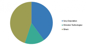
Image sensor, in today’s world, has become an important component for many devices that we use in our daily life. Smart phone and tablets are one of the most important devices that are used. The growing popularity of sharing photos over social media through mobile phones instead of carrying camera
Read More