


High-voltage DC/DC converters are widely used in industrial electronics, automotive systems, telecommunications, energy storage, battery-powered equipment and other applications where the input supply can be significantly higher than the low-voltage rails required by processors, sensors and control electronics.
Design engineers traditionally source these devices from established analog semiconductor manufacturers. However,

Power management is one of the largest and most diverse segments of the analog semiconductor market. Almost every electronic system requires some combination of DC/DC conversion, voltage regulation, battery charging, power switching, protection or power sequencing.
While companies such as Texas Instruments, Analog Devices, Infineon, STMicroelectronics, onsemi and Monolithic

IC short circuit failure analysis is the process of determining where an unintended electrical connection exists inside a semiconductor device, package or interconnect structure and identifying the physical defect that created the short.
A short circuit may initially appear only as excessive supply current, unexpectedly low resistance between two
Package failure analysis is the systematic investigation of defects and failures originating within semiconductor packaging, interconnects, solder connections, die attach, bond wires, redistribution layers and other structures that connect the semiconductor die to the outside system.
A semiconductor device may fail electrical testing even though the silicon itself is
Need semiconductor failure analysis services? AnySilicon helps semiconductor companies, fabless companies, IDMs, electronics manufacturers and engineering teams identify failure analysis laboratories with the equipment and expertise required to investigate IC, wafer, die and semiconductor package failures.
A good semiconductor failure analysis lab does more than operate laboratory equipment. The
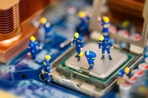
Nanoprobing is an advanced electrical characterization and fault-localization technique used in semiconductor failure analysis to directly investigate individual transistors, contacts, vias and interconnect structures inside an integrated circuit.
Instead of relying only on package-level electrical measurements, nanoprobing allows extremely small conductive structures on a deprocessed semiconductor die to be