
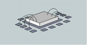
VQFN stands for Very Thin Quad Flat No-Lead, and it is best understood as a low-profile member of the QFN family rather than a fundamentally different package architecture. Like a standard QFN, a VQFN has no protruding gull-wing leads; the electrical terminals are located mainly on the bottom perimeter
Read More
QFN is usually the better choice when your priorities are minimum PCB area, short electrical paths, RF/high-frequency performance and efficient heat transfer into the PCB; QFP is usually the better choice when visible solder joints, easier optical inspection, probing and rework are more important. The fundamental difference is mechanical:
Read More
Looking for a BGA packaging company for prototype, low-volume or production semiconductor assembly?
AnySilicon helps semiconductor companies connect with IC packaging and assembly providers offering wire-bond BGA, flip-chip BGA, FCBGA, FBGA and custom substrate-based packaging services worldwide.
Submit your die, substrate, package, ball-count and production-volume requirements and
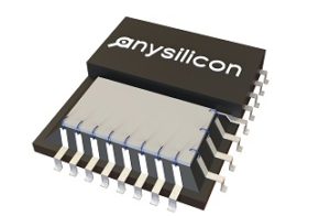
Looking for a QFN packaging company for prototype, low-volume or production assembly?
AnySilicon helps semiconductor companies connect with IC packaging and assembly providers offering standard and custom QFN packaging services worldwide.
Submit your die, package and volume requirements and AnySilicon can help identify suitable packaging partners for

Find Qualified Wafer Dicing Suppliers for Your Semiconductor Project
Wafer dicing is a critical step in semiconductor manufacturing, where processed wafers are separated into individual dies or chips before packaging, assembly, testing or further processing. The dicing process must be accurate, clean and well controlled, as poor dicing can lead
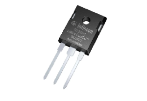
What is a TO-247 Package?
The TO-247 package is a widely used through-hole semiconductor package designed for high-power applications. It is commonly used for devices such as MOSFETs, IGBTs, diodes, and power transistors that require efficient heat dissipation and high current handling.
TO-247 stands for “Transistor Outline 247”, and