


While assembly houses are gradually becoming more and more organized in regards to following internal processes, it seems that we, their customers, are often trying to push them to make shortcuts only because “we are running out of time”.
With chip design cycle time shrinking, production related tasks such
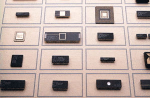
Semiconductor foundries claim they release a new technology node every two years. They may be off by a year or two, but on the whole, this is quite impressive, no doubt. Come to think of it, I don’t believe many of us even change our mobile phone every two years. How
Read More
Two years ago TSMC announced its plans to expand into IC packaging services. It is unclear how much these plans succeeded up till now, but it definitely seems that TSMC is now in an excellent position to take a big bite into the advanced IC packaging market, enter into direct competition
Read More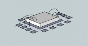
The name leadframe (or lead-frame) is actually very accurate.
Leadframe is an alloy frame that consists of the package leads and the paddle. The silicon die is attached on the paddle and the leads are connected to the die with wirebonds. That’s it.
In the above

Early on in Chip projects, yield is not taken very seriously. The common thinking goes – anyhow there isn’t much to do as this early point of time. However, there are actually several things you can do even before the Chip design starts, which will translate to clear savings.
1-
Read More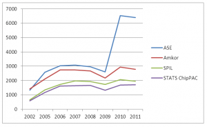
Semiconductor Assembly and Test Services are converting rapidly into a pure outsourcing mode of operation. While today perhaps only 50% of the market is using Outsourced Semiconductor Assembly and Test (OSAT, or SATS) this number is set to increase in the future.
While many of the low-end suppliers are