

TrendForce reveals that sales of advanced packaging equipment are expected to grow by more than 10% in 2024, with the potential to exceed 20% in 2025. This growth is being driven by major semiconductor manufacturers’ ongoing expansion of advanced packaging capacity and the rapidly expanding global AI server market.
Read More
Taipei, August 16 – Taiwan Semiconductor Manufacturing Co. (TSMC), the world’s largest contract chipmaker, has announced the purchase of a plant and equipment from flat panel maker Innolux Corp. for NT$17.14 billion (US$531 million). The acquisition, located in the Southern Taiwan Science Park, encompasses a 317,445 square meter facility and related
Read More
According to Yole Group, in the Advanced Packaging Market Monitor Q2 2024, advanced packaging revenue reached US$10.2 billion in Q1 2024. This quarter is anticipated to be the weakest of the year, with an 8.1% revenue decline from the previous quarter due to the seasonality that typically impacts the back-end business
Read More
Jul. 3, 2024 —- In 2016, TSMC developed and named its InFO FOWLP technology, and applied it to the A10 processor used in the iPhone 7. TrendForce points out that since then, OSAT providers have been striving to develop FOWLP and FOPLP technologies to offer more cost-effective packaging solutions.
Read More
In this guide, we’ll elucidate the pivotal role of FO-PLP in advancing the semiconductor sector. Harnessing cost-effectiveness with enhanced functionality, FO-PLP beckons a new era of electronic sophistication. Let’s delve into the ultimate guide to Fan-Out Panel-Level Packaging and explore how it’s shaping the future.
Overview of Fan-Out Panel-Level

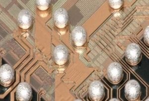
In this guide, we’ll delve into what exactly embedded die packaging is, exploring its definition, and the myriad of benefits it provides across various applications. From space-saving designs to improved heat dissipation, this innovative approach to integrating semiconductor dies is pivotal for modern electronics.
Image courtesy: ASE
Read More