

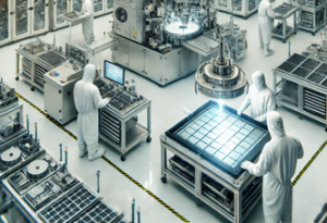
Samsung Foundry is accelerating its efforts to establish mass production capabilities for its 2nm process technology, according to industry sources. The company is actively equipping its “S3” foundry line at the Hwaseong plant, aiming for a monthly capacity of 7,000 wafers by Q1 2024. Further expansion is planned with the
Read More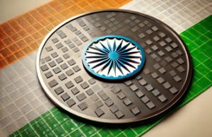
Taipei, Taiwan – October 2, 2024 – Powerchip Semiconductor Manufacturing Corporation (PSMC), a leading Taiwanese foundry, has announced a strategic shift in its global expansion plans, opting to scrap a previously announced semiconductor fab project in Japan in favor of building a new fab in Gujarat, India. The decision comes
Read More
Tokyo, Japan – October 2, 2024 – Toppan Photomask, a global leader in the semiconductor photomask industry, will officially change its name to Tekscend Photomask on November 1, 2024. The rebranding represents a strategic move to reflect the company’s ongoing commitment to technological innovation and growth as a premier photomask
Read MoreThe European Commission has approved Poland’s plan to provide over 7.4 billion zlotys ($1.91 billion) in state aid to support Intel’s construction of a new semiconductor assembly and test facility near Wroclaw. This green light marks a significant step forward in the project, which is expected to be finalized by
Read More
Seoul, South Korea – [Sep 14, 2024] – SK Keyfoundry, the dedicated logic foundry unit of SK Hynix, continues to expand its footprint in the specialty foundry market. The company has recently announced the launch of its fourth-generation 180nm Bipolar-CMOS-DMOS (BCDMOS) process, further strengthening its technological capabilities in power-demanding applications
Read More
Vanguard International Semiconductor Corp (VIS) and Episil Technologies Inc. announced today a strategic partnership to build an 8-inch silicon carbide (SiC) wafer fabrication facility in Taiwan. The collaboration, facilitated by an equity acquisition deal, will see VIS acquire a 13% stake in Episil for NT$2.48 billion (US$77.1 million).
The