

Hsinchu, Taiwan, R.O.C., May 15, 2020 – TSMC (TWSE: 2330, NYSE: TSM) today announced its intention to build and operate an advanced semiconductor fab in the United States with the mutual understanding and commitment to support from the U.S. federal government and the State of Arizona.
This facility,
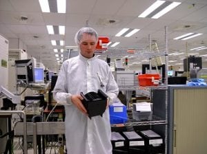
Semiconductors are extremely critical and central components in modern technology. Most of the electronic devices we use today operate on these integrated circuits that are housed on silicon wafer chips. It does, however, take a lot of processing and work to get the semiconductor in that condition from the raw
Read More
Over the past decade, the IC industry has been paring down its older capacity as manufacturers have consolidated or transitioned to the fab-lite or fabless business models. In its recently released Global Wafer Capacity 2020-2024 report, IC Insights shows that due to the surge of merger and acquisition activity in the middle
Read More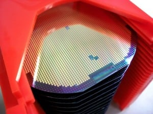
The success and proliferation of integrated circuits has largely hinged on the ability of IC manufacturers to continue offering more performance and functionality for the money. Driving down the cost of ICs (on a per-function or per-performance basis) is inescapably tied to a growing arsenal of technologies and wafer-fab manufacturing
Read More
GLOBALFOUNDRIES, abbreviated as GF, is a semiconductor foundry based in Santa Clara, California in the United States. GLOBALFOUNDRIES, is responsible for the mass manufacturing of integrated circuits for popular and successful semiconductor companies including but not limited to the likes of Qualcomm, NXP and STMicroelectronics.
The Formation Of GLOBALFOUNDRIES
Read More
January 21, 2020: CMC Microsystems has signed an agreement with GLOBALFOUNDRIES® (GF®), the world’s leading specialty foundry, that will provide access to GF’s advanced and specialized FinFET, RF SOI, FDX, SiGe, and Silicon Photonics platforms for CMC researchers at more than 60 Canadian universities and colleges, in addition to
Read More