

For decades, electronics product innovation has been incremental in nature, relying largely on the next generation of semiconductors to deliver performance improvement. For almost 50 years Moore’s Law has delivered 2x performance (power or cost) improvement in semiconductors every 18 months, outpacing any product or system level innovation cycle that could be achieved by even the most ambitious hardware teams. What has evolved is a “sit & wait” approach, to product innovation. However it is now clear that Moore’s law is broken, and the implications are profound for hardware designers.
The Semiconductor industry is consolidating, into fewer huge players. The fabless model is under increasing strain favouring only the most massively distributed companies. Hardware product teams can no longer “sit & wait” for performance improvement to be delivered by semiconductor companies, architecture is becoming more relevant, it becomes feasible – even necessary, for product teams to develop their own custom ASIC designs.
Here, I highlight some of the trends that have caused the hardware industry to favour a “sit & wait” approach to innovation, and looking forward 5 to 10 years, suggest what will be a fundamental shift in how hardware product innovation happens.
Moore’s Law has been relentless for almost 50 years
A new hardware product has to be conceived, designed, prototyped, validated, mass manufactured, and distributed to enable traction and ultimately wide scale adoption by end users. A typical product innovation cycle, which can take 2-3 years to complete.
In the past, Moore’s law will have delivered 2 cycles of process node shrinks in that same time frame, each of which delivering a 2x improvement, in performance, power, cost. This makes it impossible for hardware designers to outpace Moore’s law using any other innovation approach. What has emerged as a result, is a “sit & wait” approach to innovation from product companies.
For semiconductor companies in turn to be competitive in the Moore era, increasingly required massive distribution and infrastructure to deploy millions of units per month. This favoured businesses only on the largest scale, and led to the adoption and evolution of the current fabless semiconductor model.
As the complexity of each new process node grew however, to maintain the pace of Moore’s law, fabless semi companies needed to have two or three generations in development simultaneously, compounding the requirement of massive scale, and ultimately driving the consolidation we have been seeing since the beginning of the current decade.
Moore’s Law is slowing down
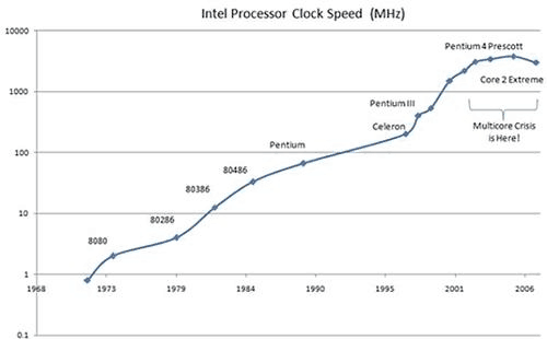
Arguably clock scaling as a performance metric, ended in 2003, since then multi-core architectures have been employed to achieve the performance gains predicated on Moore’s Law, as shown in the graph below.
Certain fundamental parameters have already hit a wall, such as Vth, Vddmin, Gate Oxide thickness.
This is not to say that scaling will not happen, it certainly will at least to possibly 5nm, somewhere between 2020 and 2030 (H. Lwai Microelecton. Eng 2009 , doi:10.1016/j.mee.2009.03.129), and there will still be some applications with unit volume sales that support the economics required.
However, we are not getting 2x improvements every 18th months, and this has profound implications for hardware innovation, as the “sit & wait” approach to hardware and product innovation falls apart.
The key insight is, when you look at a typical 2-3 year product development timeline, in the post Moore era, there is ample time to execute this cycle in between process node releases. As a result there is now a compelling reason and time, to consider new innovative system architectures or build custom ASICs optimised for a specific product, since doing so beats the improvement that can be gained from process scaling alone.
In the post Moore’s law world, architecture matters, optimisation matters, and a custom ASIC approach is beginning to re-emerge, as not just feasible, but a necessary option for many System Companies and OEMs.
In other words, there is a genuine market window for monetizing innovative product and hardware solutions, based on custom ASICs, instead of “sit & wait”.
Deceleration of Moore’s Law is already showing its impact on markets that are not as sensitive to performance. Consider the rise of the Arduino platform. The Arduino took several years to gain popularity, with virtually the same hardware at its core since 2005.
Closer to home, consider the Iridium Satellite transceiver platform, S3 Group have developed 3 generations of custom RF & mixed signal ASIC solutions, in the same period as two process node developments, enabling Iridium and more importantly their customers benefit in terms of cost & form factor through innovative new architecture approaches, rather than process shrinks of the original ASSPs.
In what are now mature process nodes, ASIC development times are shortened considerably due to the availability of semiconductor IP, production proven on those nodes. As the process node shrink cycle lengthens, typical Product Development cycle now outperforms the process node cycle in delivering price/performance improvements.
In the past there was little motivation to optimise hardware or architecture, when gains could be made by cramming more features into software, waiting for a semiconductor upgrade cycle and then it would start to run well as Moore’s Law delivered semiconductor performance. Remember how slow WinXP and Vista ran when they first came out?
Megatrends like open compute project, the maker movement, hardware hackathons, are all examples of (or reactions to) the realisation that gains from product architecture optimisation can and do outpace those of semiconductor upgrades.
In the post Moore’s law world, architecture matters, hardware optimisation matters, doing custom ASICs are not just feasible, but a necessary option for many System Companies and OEMs.
As process technology nodes advance and Moore’s Law slows at the leading edge, falling costs & increasing capacity on more mature nodes, coupled with the availability of high performance RF & Mixed Signal IP is enabling a new paradigm in Hardware and Product Innovation. OEMs can now embark on custom ASIC developments to take advantage of higher levels of integration, realising significant BOM savings.
While the open hardware movement, and open compute project are still niche areas and for now custom ASICs are maybe out of reach, other megatrends like IoT are driving new platforms, architectures and opportunities. Not in over 30 years, have custom, mixed signal, ASIC developments been within reach of so many lower volume hardware applications.
__________________________________________________________________
Guest blogger Donnacha O’Riordan, Director of Services Strategy for S3 Group
This article first appeared on EE Times’ Planet Analog website.


