

In this article we will discuss extrinsic semiconductors. In short extrinsic semiconductors are devices that have been doped with specific chemicals. This process helps modifying the electrical properties of a relatively pure semiconductor crystal.
Intrinsic (pure semiconductor) or un-doped semiconductors have free electrons and holes. Both of them are generated in pairs because they are thermally generated and are equal in numbers. The current in a semiconductor contains both holes and electrons. But semiconductors don’t conduct current well because:
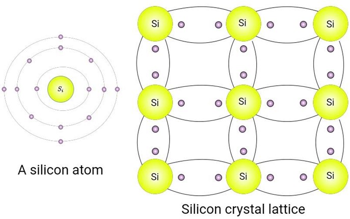
Figure 1: A Silicon Atom and its Crystals
Contrarily, in a metal conductor, each metal atom releases an electron that helps to conduct current. In a conductor made of metal, there are exactly as many atoms as free electrons. Therefore, there are a lot of electrons moving through a conductive material.
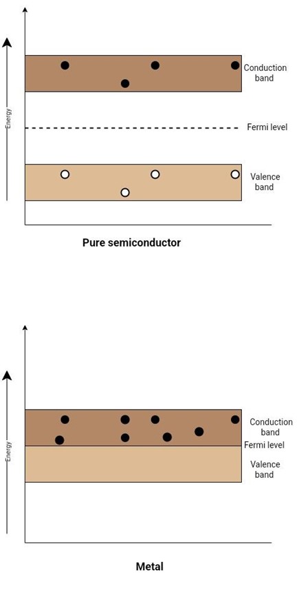
Figure 2: Band Diagram of Metal and an Intrinsic (pure semiconductor)
By increasing the number of holes or electrons, pure silicon or germanium can be altered to increase conductivity. The pure silicon material is put through a process in which impurities are carefully added to increase the number of charged carriers (either holes or electrons). This practice is known as doping.
To increase the number of free electrons in pure silicon material, it goes through a doping process and a pentavalent impurity is added. The pentavalent elements, arsenic and phosphorus, are used for this purpose. They have five valence electrons each and are hence known as pentavalent elements. Let’s examine a silicon atom in a crystal. Each atom has four valence electrons. Each electron is covalently bonded with an electron. So each silicon atom is surrounded by eight electrons in a crystal lattice. When a pentavalent element is added as a dopant, the structure of the crystal changes a little. The effect of this doping process is given below:
There are five valence electrons in pentavalent elements. Each Valence electron is covalently bonded with four other atoms. The fifth electron remains free and contributes to enhanced conductivity. It becomes a conduction band electron since it is not associated with any covalent bond. The pentavalent atom is also known as the donor atom because it donates a free electron.
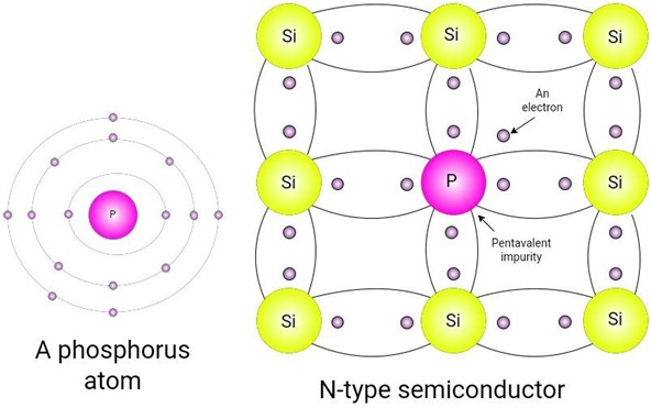
Figure 3: A Phosphorus Atom and N-type Semiconductor
The change in conductivity after doping is observed by looking at the band diagram. An extra energy level called the donor level is created for these electrons (free electrons result in doping). This level is created just below the conduction band. In the case of heavy doping, it overlaps with the conduction band. It is at a distance of 0.05 eV to 0.1 eV from the conduction band. So, an electron only requires 0.05–0.1 eV to jump into the conduction band. This energy is readily available at room temperature.
In other words, at 0K, there are many electrons in the conduction band, while the valence band has no holes. The electrons occupying the donor level promptly jump into the conduction band even at room temperature. Now it is even more difficult for electrons to jump from the valence band to the conduction band through thermal agitation. In this case, the fermi level is closer to the conduction band because the probability of finding an electron near the edge of the conduction band is larger than the probability of finding a hole at the valence band edge.
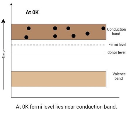
Figure 4: Position of the fermi level and effect of a donor impurity in an n-type extrinsic semiconductor
In n-type semiconductors, the majority of carriers are electrons. The holes are in minority carriers and neglect the flow of current because of minority carriers. Consider an n-type material, and connect a battery across it. The figure below depicts the conduction process in an n-type semiconductor.
The negatively charged electrons will be attracted towards the positive terminal of the battery and will flow through the wire.
Similarly, positively charged holes will start moving towards the negative terminal of the battery. These holes will attract electrons from the negative terminal. In this way, current flows in a semiconductor bar.
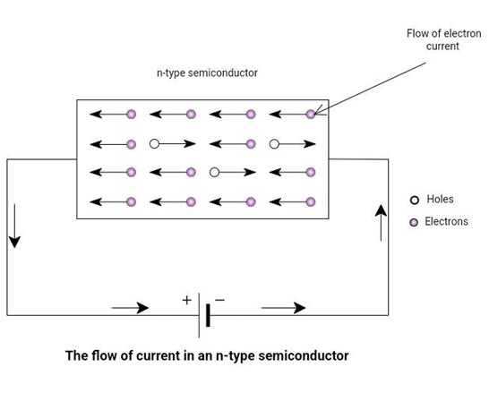
Figure 5: The flow of current
At 0K, the fermi level lies exactly in between the donor level and the bottom of the conduction band.
As the temperature increases, electrons are created because of thermal agitation. The donor level will be filled with more and more electrons. As the saturation temperature occurs, the fermi level coincides with the donor level.
With the increasing temperature, the number of electrons produced by thermal agitation becomes greater than electrons from impurity elements. In this case, the n-type semiconductor loses its extrinsic behavior and behaves as an intrinsic semiconductor. As the temperature increases, the fermi level starts moving towards the center of the band gap.
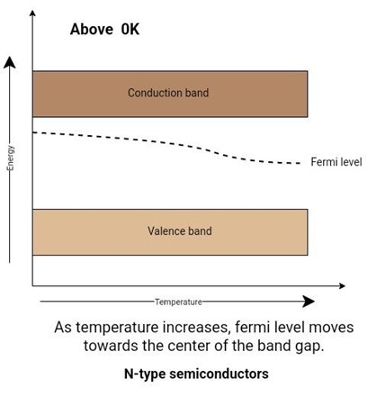
Figure 6: Effect of temperature on fermi level
To increase the number of holes in pure silicon material, it goes through a doping process and a trivalent impurity is added. Boron is used for this purpose. It has three valence electrons and is hence known as a trivalent element. When a trivalent element is added as a dopant to the pure silicon crystal, its structure changes a little. The effect of this doping process is given below:
There are three valence electrons in trivalent elements. Each valence electron is covalently bonded with three other atoms. The fourth covalent bond lacks an electron; it has a hole instead. This hole can be filled with free electrons. The energy to fill this position is 0.01 eV. The trivalent atom is also known as the acceptor atom because it accepts an electron at this position.
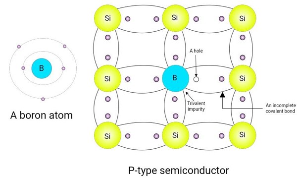
Figure 7: a boron atom and p-type semiconductor
The change in conductivity after the doping is observed by looking at the band diagram. An extra energy level called the acceptor level is created for these holes (holes result in doping). This level is created just above the valence band. In the case of heavy doping, this level overlaps with the valence band. The acceptor level is at a distance of 0.01-0.5 eV from the valence band. So, an electron in the valence band only needs 0.01-0.5 eV of energy to jump into an acceptor level and occupy a hole there.
In other words, at 0K, there are no free electrons in the conduction band. The valence band has many holes due to doping. At room temperature, there is enough thermal energy to produce some free electrons. An electron from the neighboring atoms can jump into the hole. It will create a hole in a new place.
Now an electron in the valence band doesn’t need to go to the conduction band. An energy level (that is, acceptor level) is close to the valence band.
In this case, the fermi level is closer to the valence band because the probability of occupation of energy levels by the holes in the valence band is greater than the probability of occupation of energy levels by electrons in the conduction band.
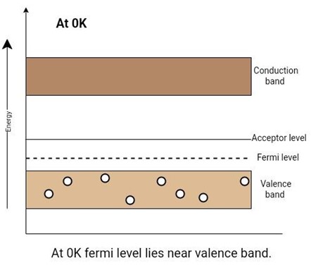
Figure 8: Position of the fermi level and effect of an acceptor impurity in a p-type extrinsic semiconductor
In p-type semiconductors, the majority of carriers are holes. The electrons are minority carriers. We neglect the flow of current because of minority carriers. Consider a p-type material, and connect a battery across it. The figure below depicts the conduction process in a p-type semiconductor.
The negatively charged electrons will be attracted towards the positive terminal of the battery and will flow through the wire.
Similarly, positively charged holes will start moving towards the negative terminal of the battery. These holes will attract electrons from the negative terminal. In this way, current flows in a semiconductor bar.
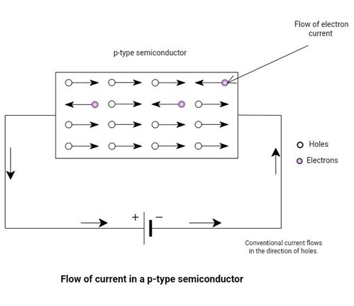
Figure 9: The flow of current
At 0K, the fermi level lies exactly in between the acceptor level and the top of the valence band.
As the temperature increases, holes are created because of thermal agitation. The acceptor level will be filled with more and more holes. As the saturation temperature occurs, the fermi level coincides with the acceptor level.
With the increasing temperature, the number of holes produced by thermal agitation becomes greater than the holes from impurity elements. In this case, the p-type semiconductor loses its extrinsic behavior and behaves as an intrinsic semiconductor. As the temperature increases, the fermi level starts moving towards the center of the band gap.
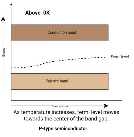
Figure 10: Effect of temperature on fermi level


