



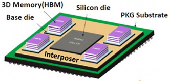
SK hynix has broken ground on a major advanced packaging facility in Indiana as the memory manufacturer expands production capacity to meet rapidly growing demand for High Bandwidth Memory driven by artificial intelligence.
South Korean memory manufacturer SK hynix has started construction of its first HBM production base in the United States, marking another major investment in the rapidly expanding AI semiconductor supply chain. The company held a groundbreaking ceremony on August 27 for the facility in West Lafayette, Indiana. SK hynix plans to invest more than $4 billion in the project, which will combine high-volume advanced packaging and testing of next-generation HBM with an advanced packaging research and development center.
The approximately 133-acre site is expected to become one of the most important HBM manufacturing and packaging locations in the United States. SK hynix expects the facility’s first cleanroom to open by October 2028, with mass production of next-generation HBM scheduled to begin during the second half of 2029. Once fully operational, the facility is expected to employ approximately 1,000 people directly. SK hynix estimates that the broader project could support around 7,000 direct and indirect jobs and involve more than 100 ecosystem partners.
The Indiana facility represents an important expansion of SK hynix’s manufacturing footprint outside Asia. Unlike a conventional front-end DRAM wafer fab, the Indiana facility will operate in close coordination with SK hynix’s manufacturing plants in South Korea. Advanced memory wafers manufactured in Korea will be shipped to Indiana, where they will undergo advanced packaging and testing before being supplied to U.S. customers as locally produced HBM products.
HBM has become one of the semiconductor industry’s most strategically important products as AI accelerators require increasingly large amounts of high-speed memory located close to the processor. HBM achieves significantly higher bandwidth than conventional DRAM by vertically stacking multiple DRAM dies and connecting them using advanced interconnect technologies. Growing deployments of AI accelerators for data centers have consequently created unprecedented demand for HBM.
SK hynix will also establish an Advanced Packaging R&D Testbed alongside the Indiana production operation. The center will allow SK hynix to collaborate with customers, universities and semiconductor ecosystem partners on future packaging technologies.
The R&D facility is intended to support areas including:
→ Next-generation HBM packaging
→ Advanced semiconductor integration
→ Prototype manufacturing
→ Package performance validation
→ New system-level packaging technologies
Advanced packaging has become increasingly important as traditional semiconductor scaling becomes more difficult and expensive. Technologies including chip stacking, heterogeneous integration and chiplets are allowing semiconductor companies to increase system performance without depending exclusively on transistor scaling.
SK hynix has also signed a memorandum of understanding with Purdue University covering research and development in advanced packaging. Purdue’s proximity to the new facility is expected to provide SK hynix with access to semiconductor research capabilities as well as a pipeline of engineering talent. The collaboration is expected to focus on next-generation advanced packaging technology and broader semiconductor research.
The relationship between manufacturing, R&D and university research could eventually make West Lafayette an important U.S. center for advanced memory packaging.
The investment comes during an extraordinary expansion of the global memory industry. AI infrastructure is consuming increasing amounts of HBM as companies deploy larger GPU and AI accelerator clusters.
HBM has become particularly important because the performance of AI processors increasingly depends not only on computational capability but also on how quickly large volumes of data can move between memory and processors. This has created strong demand for HBM from companies developing AI accelerators and data-center infrastructure.
SK hynix has emerged as one of the major beneficiaries of this transition and has been aggressively expanding its manufacturing infrastructure to secure additional capacity.
The Indiana investment is only one component of a much larger SK hynix capacity expansion. In August, the company approved approximately 54 trillion won of investment for two additional semiconductor manufacturing projects in South Korea. The investment will be divided between the Yongin Y2 DRAM fab and Cheongju M17 NAND fab. Approximately 35.2 trillion won will be invested in Y2, while around 19.1 trillion won will be allocated to M17.
Y2 will become the second of four semiconductor fabs planned for SK hynix’s massive Yongin Semiconductor Cluster. The facility will primarily support DRAM production and will occupy approximately 1.13 million square meters of floor area. Construction is expected to begin in July 2027.
SK hynix plans to open the facility’s first cleanroom in June 2029, with the site eventually supporting production of HBM and next-generation DRAM. Construction of the first Yongin facility, Y1, is already underway, with its initial cleanroom scheduled to open in early 2027. The Yongin cluster is expected to become one of SK hynix’s most important long-term semiconductor production centers.
SK hynix is simultaneously expanding its NAND flash manufacturing infrastructure. The company plans to construct the new M17 fab at its Cheongju campus, which already contains the M11, M12 and M15 production facilities. M17 will occupy approximately 680,000 square meters. Construction is expected to begin in February 2027, with the first cleanroom scheduled to open in December 2028.
The facility will provide SK hynix with additional NAND production capacity as the company prepares for future growth in storage demand associated with AI infrastructure and data centers.
The scale of SK hynix’s investments highlights how dramatically AI is reshaping the memory semiconductor industry. AI processors receive much of the attention surrounding the current semiconductor boom, but memory capacity and advanced packaging are becoming equally critical components of AI infrastructure. Without sufficient HBM bandwidth, even the most powerful AI processors cannot operate at their full potential.
That has transformed advanced memory technologies from relatively conventional semiconductor components into strategic parts of the AI supply chain. SK hynix is responding by simultaneously expanding DRAM wafer production, NAND capacity and advanced HBM packaging. Its emerging manufacturing network will stretch from Icheon, Cheongju and Yongin in South Korea to West Lafayette in the United States.
With HBM demand continuing to expand alongside AI infrastructure investment, the Indiana project could become an increasingly important component of the U.S. semiconductor ecosystem when production begins in 2029.
| Segment | Period | Rank | Company | Revenue (US$M) | Previous Revenue (US$M) | QoQ Growth | Market Share | Previous Market Share |
|---|---|---|---|---|---|---|---|---|
| DRAM | 1Q26 | 1 | Samsung | 37,323 | 19,300 | 93.4% | 38.5% | 36.0% |
| DRAM | 1Q26 | 2 | SK hynix | 27,982 | 17,221 | 62.5% | 28.8% | 32.1% |
| DRAM | 1Q26 | 3 | Micron | 21,750 | 11,975 | 81.6% | 22.4% | 22.4% |
| DRAM | 1Q26 | 4 | Nanya | 1,552 | 970 | 60.0% | 1.6% | 1.8% |
| DRAM | 1Q26 | 5 | Winbond | 568 | 297 | 91.4% | 0.6% | 0.6% |
| DRAM | 1Q26 | 6 | PSMC | 43 | 33 | 29.9% | 0.0% | 0.1% |
| DRAM | 1Q26 | — | Others | 7,783 | 3,782 | 105.8% | 8.0% | 7.1% |
| DRAM | 1Q26 | Total | 97,000 | 53,578 | 81.0% | 100.0% | 100.0% | |
| 2Q26 NAND Flash Revenue Ranking | ||||||||
| NAND Flash | 2Q26 | 1 | Samsung | 23,059.3 | — | 70.7% | 29.3% | 31.6% |
| NAND Flash | 2Q26 | 2 | SK hynix Group (SK hynix + Solidigm) | 14,272.9 | — | 89.5% | 18.2% | 17.6% |
| NAND Flash | 2Q26 | 3 | Micron | 11,850.0 | — | 99.2% | 15.1% | 13.9% |
| NAND Flash | 2Q26 | 4 | Kioxia | 10,723.0 | — | 79.9% | 13.6% | 13.9% |
| NAND Flash | 2Q26 | 5 | SanDisk | 8,965.0 | — | 50.7% | 11.4% | 13.9% |
| NAND Flash | 2Q26 | Total Top 5 | 68,870.2 | — | 77.0% | 87.6% | 90.9% | |
Source: TrendForce, June–August 2026. DRAM previous-period data refers to 4Q25. NAND Flash previous market share refers to 1Q26.