

Get the semiconductor daily news directly to you by subscribing to our email list. For ASIC designer and managers, staying updated with the latest news, technologies, and trends is crucial. Here are the lastest news from the semiconductor industry.
Introduction
Low power test efforts in SOC design are broadly classified into – fine tuning ATPG patterns, enhancing collaterals for supporting low power ATPG, architecture for low power DFT, improving estimation and correlation. The flow discussed here comes under the category of “fine tuning ATPG patterns”.
Currently due

GlobalFoundries is downsizing at its semiconductor plant in Germany by 20 percent, according to several newspapers in Germany.
GlobalFoundries has factories in Germany, Singapore and the USA. The “Fab 1” in Dresden is one of the largest private employer in the city. The plant is equipped with a clean room
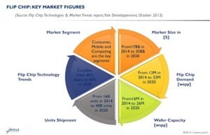
Flip Chip technology is expected to reach $25 billion market value and wafer demand of 32 million (12”eq.wafers) in 2020, supported by the wider adoption of Cu pillar technology. That growth will be led by Moore’s law pushing beyond the 28nm node and ‘More than Moore’ evolution in next generation
Read More
Mergers and acquisitions happen very frequently in the semiconductor industry. However, what it is not common that these kind of operations proceed smoothly, quickly and without hurdles. This is the case of the public takeover of Siliconware Precision Industries (SPIL) for Advanced Semiconductor Engineering Inc (ASE). Indeed, the company dealing
Read More
We all know that solar energy will face a positive growth in the next future. However, Leading IC foundry Taiwan Semiconductor Manufacturing Co. Ltd. (Hsinchu, Taiwan) is moving countertrend by announcing its intent of quitting the solar energy subsidiary activity with TSMC.
Indeed, the big foundry is expecting to
According to the latest report released by IC Insights, Global Wafer Capacity 2015-2019 shows a delay in 450mm wafers’ development and production in contrast to an increased 300mm wafers’ consumption by technology companies.
Judging from statistics, in fact, despite the huge economic incentives that would be generated on the

GlobalFoundries is probably doing something right because China has set its eyes on GlobalFoundries with rumors of a possible imminent acquisition. Indeed, thanks to several strategical decisions, GlobalFoundries is offering today a unique portfolio, both CMOS and SiGe processes, cutting-end technology (14nm and 22FDSOI) and a global semiconductor manufacturing footprint.
Read More

AnySilicon, the semiconductor vendors marketplace and IP portal reveals today its official website ranking measured by Alexa.com the global leader in website analytics.
In the past ChipEstimate and Design-Reuse were the only players in the IP portal market. But in Jan-2015 AnySilicon has launched a new IP portal in

Thanks to the $30 million investment made through government funding, the American Defence Advanced Research Projects Agency (DARPA) is set to start a new program that will enable a significant cut down of costs for custom integrated circuits for specific tasks (ASIC).
The revolutionizing program will be called CRAFT

The 52nd Annual Design Automation Conference (DAC52) at San Francisco’s Moscone Centre had a number of interesting power management announcements, making this one of the hottest topics of the show. SureCore unveiled its own low power SRAM technology, creating a great deal of interest and setting a new low power
Read More