


The history of GlobalFoundries is a story about one of the semiconductor industry’s most important transformations: the separation of chip design from semiconductor manufacturing.
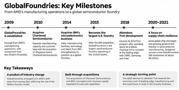
Established in 2009 following the separation of AMD’s manufacturing operations, GlobalFoundries entered the market with an ambitious objective: to become a major competitor to Taiwan Semiconductor Manufacturing Company (TSMC) and Samsung.
Backed by investors from Abu Dhabi, the company acquired semiconductor fabrication facilities, expanded its global manufacturing operations and invested heavily in advanced process technologies.
However, despite substantial investments and technological partnerships, GlobalFoundries eventually discovered that competing at the leading edge of semiconductor manufacturing required financial resources and production volumes that only a handful of companies could sustain.
Its decision in 2018 to abandon development of its 7nm process marked a turning point not only for the company but also for the global semiconductor industry.
The origins of GlobalFoundries can be traced to Advanced Micro Devices (AMD), founded in 1969 by Jerry Sanders and a group of former Fairchild Semiconductor employees.
During the early decades of the semiconductor industry, most major chip companies followed an integrated business model. They developed semiconductor products and manufactured those products in their own fabrication facilities, commonly known as fabs.
AMD was no exception.
Jerry Sanders strongly believed that semiconductor manufacturing was an essential part of a successful chip company. His commitment to owning fabrication facilities became associated with the famous phrase:
“Real men have fabs.”
For Sanders and other early semiconductor executives, controlling manufacturing was closely connected to technological independence and competitiveness. However, by the 1990s and 2000s, the economics of semiconductor manufacturing were changing.
Each new generation of process technology required more sophisticated equipment, greater manufacturing precision and significantly higher capital investments. A fabrication facility capable of producing advanced logic chips could cost billions of dollars.
For companies such as AMD, competing simultaneously in semiconductor design and advanced manufacturing was becoming increasingly difficult. Meanwhile, the success of TSMC demonstrated that a different business model was possible.
Rather than designing its own chips, TSMC manufactured semiconductors for external customers. By producing chips for many different companies, it could spread its enormous manufacturing investments across a larger customer base. This model would eventually challenge AMD’s long-standing approach.
Following Jerry Sanders’ departure from AMD, the company’s leadership reconsidered the financial burden of owning advanced semiconductor fabrication facilities.
The separation of design and manufacturing increasingly appeared to offer a way forward. AMD eventually announced that it would divide its chip design and manufacturing businesses. Its manufacturing facilities would become part of a newly established foundry company, supported by investment from Abu Dhabi. Mubadala, an investment arm of the Abu Dhabi government, became the principal investor. The transaction received approval from the Committee on Foreign Investment in the United States (CFIUS), which determined that the investment did not present national security concerns.
In 2009, GlobalFoundries emerged as an independent semiconductor manufacturer. The company inherited AMD’s substantial manufacturing facility in Germany and was developing a new advanced semiconductor fabrication facility in New York. Unlike AMD, GlobalFoundries would operate as a foundry, manufacturing chips for multiple semiconductor design companies rather than exclusively for one customer.
The new company entered a market dominated by TSMC, with Samsung also emerging as an important competitor in contract semiconductor manufacturing.
When GlobalFoundries was established, industry analysts believed it had a genuine opportunity to challenge the established foundries. Several factors appeared to favor the new company.
First, GlobalFoundries inherited significant semiconductor manufacturing expertise and existing fabrication infrastructure from AMD. Second, the company was developing advanced manufacturing capacity in Germany and the United States, giving it a different geographic manufacturing footprint from its Asian competitors.
Third, GlobalFoundries was working with IBM and Samsung on semiconductor technology development. These relationships offered a potential advantage as the industry transitioned toward increasingly complex transistor technologies. There was also considerable demand among fabless semiconductor companies for an alternative to TSMC.
By this period, TSMC controlled approximately half of the global foundry market. Although Samsung possessed advanced semiconductor manufacturing technology, some potential foundry customers were concerned about the company’s competing consumer electronics businesses.
GlobalFoundries, like TSMC, did not have the same conflict of interest with customers whose products it manufactured. Furthermore, TSMC was experiencing manufacturing difficulties with its 40nm process technology around 2009, creating an opportunity for competing foundries.
The global financial crisis of 2008–2009 had also disrupted semiconductor demand, introducing uncertainty into the industry’s competitive landscape. For GlobalFoundries, the combination of new investment, technological partnerships and changing market conditions created an opportunity to establish itself as a major semiconductor manufacturing company.
Despite its manufacturing capabilities, GlobalFoundries remained significantly smaller than its major competitors. The company needed to expand its production capacity and customer base.
One of its first major steps was the acquisition of Chartered Semiconductor, a Singapore-based semiconductor foundry, in 2010. Chartered Semiconductor had already established itself as an important contract manufacturer serving external semiconductor customers.
Its acquisition provided GlobalFoundries with additional manufacturing capacity and a stronger position in the global foundry market. A second major expansion followed in 2014, when GlobalFoundries acquired IBM’s microelectronics manufacturing business.
IBM had played an important role in the development of semiconductor technology for decades. However, IBM faced the same economic challenge that had led AMD to separate its manufacturing operations. Maintaining advanced semiconductor fabrication facilities demanded enormous capital investment, while other parts of IBM’s business offered more attractive financial opportunities.
Rather than investing billions in new fabrication facilities, IBM decided to leave semiconductor manufacturing and concentrate resources elsewhere. GlobalFoundries agreed to acquire its microelectronics business and manufacture chips for IBM. These acquisitions transformed GlobalFoundries into one of the world’s largest semiconductor foundries. By 2015, the company had become the largest foundry operating in the United States. Nevertheless, it remained much smaller than TSMC.
By 2015, GlobalFoundries had become a significant competitor in the semiconductor foundry industry. However, the difference in scale between GlobalFoundries and TSMC remained considerable.
| Company | Approximate foundry market share in 2015 |
|---|---|
| TSMC | More than 50% |
| GlobalFoundries | Approximately 10% |
| UMC | Approximately 10% |
| Samsung Foundry | Approximately 5% |
Samsung’s relatively small share of the contract foundry market did not reflect its total semiconductor manufacturing capacity, because Samsung also produced substantial volumes of chips for its own products. In terms of overall wafer manufacturing capacity, approximately 2.5 million wafers per month for Samsung, 1.8 million for TSMC and 700,000 for GlobalFoundries at the time.
These differences mattered enormously. Semiconductor manufacturing is a business in which scale can provide substantial economic and technological advantages. Higher production volumes allow companies to spread equipment and development costs across more wafers.
Manufacturing experience can also contribute to improved yields, greater process stability and more efficient production. For GlobalFoundries, competing with a much larger foundry such as TSMC required continuous investments in technology despite having a smaller manufacturing base over which to recover those costs.
As GlobalFoundries attempted to expand, semiconductor manufacturing technology was undergoing a fundamental transformation. For decades, the industry had increased semiconductor performance by making transistors progressively smaller.
This development followed the trend commonly known as Moore’s Law. During the 2000s, manufacturers advanced through process generations such as 180nm, 130nm, 90nm, 65nm and 45nm. However, continued transistor scaling became increasingly difficult. As transistors became smaller, leakage currents and other physical effects began to create significant challenges. The semiconductor industry responded by developing new transistor architectures.
One of the most important innovations was the FinFET transistor, which introduced a three-dimensional structure to improve control over electrical current. FinFET technology enabled continued scaling, but manufacturing these structures required extremely precise deposition, etching and lithography processes.
For GlobalFoundries, the transition to more advanced transistor architectures presented both an opportunity and a major technological risk. The company experienced difficulties developing its 28nm manufacturing process.
To reduce the risk of further delays, GlobalFoundries decided to license a 14nm process technology from Samsung rather than develop the process entirely in-house. This arrangement provided access to advanced transistor technology while reducing some of the development challenges. Nevertheless, the next generation of semiconductor manufacturing would prove even more demanding.
During the 2010s, leading semiconductor manufacturers began preparing for process technologies requiring extreme ultraviolet (EUV) lithography. EUV lithography promised to enable the fabrication of smaller semiconductor features beyond the practical limitations of existing lithography methods.
However, the technology was extraordinarily difficult to develop. EUV equipment required sophisticated optical systems, specialized light sources and extraordinary manufacturing precision. TSMC, Intel and Samsung were investing heavily in the technology, believing it would be necessary to remain competitive in advanced semiconductor manufacturing.
GlobalFoundries also prepared to introduce EUV technology as part of its planned 7nm process. The company invested substantial resources in developing the technology and acquired EUV lithography equipment for its advanced Fab 8 facility. By 2018, GlobalFoundries had already spent approximately $1.5 billion developing its planned 7nm process.
Bringing the technology into production would have required an additional investment of roughly the same magnitude. For a company with considerably less manufacturing capacity than TSMC or Samsung, the financial risk was enormous. The question was no longer simply whether GlobalFoundries could develop the technology.
It was whether the company could generate enough production volume and revenue to justify the investment.
In 2018, GlobalFoundries made one of the most consequential decisions in its history. The company canceled its EUV development program and abandoned plans to introduce a 7nm process. The decision marked its withdrawal from the competition to manufacture the industry’s most advanced logic chips.
GlobalFoundries had concluded that the investment required to develop 7nm manufacturing could not be justified by its financial resources and expected production scale. Rather than continuing to compete directly with TSMC, Intel and Samsung at the leading edge, the company redirected its manufacturing strategy.
GlobalFoundries also reduced its research and development spending by approximately one-third. The decision illustrated a fundamental economic reality of advanced semiconductor manufacturing. Even a company supported by wealthy investors and possessing substantial manufacturing expertise could struggle to finance the next generation of process technology.
The cancellation also reduced the number of companies pursuing leading-edge logic manufacturing from four to three. TSMC, Samsung and Intel remained committed to developing increasingly advanced process technologies. GlobalFoundries had chosen a different direction.
The decision to withdraw from leading-edge process development did not eliminate the need for GlobalFoundries’ manufacturing capabilities. Not every semiconductor application requires the smallest available transistor geometry. Semiconductor products can be divided into different categories with different technological and economic requirements.
Advanced logic processors and memory devices often depend heavily on continued improvements in transistor density. However, many other semiconductor applications have different priorities. Analog circuits, radio-frequency devices, sensors and power-management semiconductors often rely on technologies in which specialized device characteristics and circuit design are more important than aggressive transistor scaling.
These technologies can be manufactured using process generations that are less expensive to develop and maintain than the most advanced logic nodes. This distinction helps explain the strategic significance of GlobalFoundries’ decision.
Instead of competing in a race that demanded increasingly enormous capital investments, GlobalFoundries could continue operating established manufacturing technologies without pursuing every new generation of transistor scaling. The company’s history therefore demonstrates that semiconductor manufacturing competitiveness cannot be measured solely by transistor dimensions.
Production economics, process reliability, manufacturing expertise and customer requirements also play important roles.
GlobalFoundries’ history also reflects the internationalization of semiconductor manufacturing. The company originated from AMD’s manufacturing operations in Germany, expanded into the United States and acquired manufacturing capacity in Singapore.
Its financing involved investors from Abu Dhabi, while its technology partnerships connected it with major semiconductor companies in the United States and South Korea.
These relationships demonstrate how semiconductor manufacturing became an increasingly global business.
The global chip shortages of 2020–2021 highlighted the vulnerability of semiconductor supply chains. Countries sought to attract new manufacturing investments and reduce their dependence on geographically concentrated production.
This development reflected continued government interest in expanding semiconductor manufacturing capacity, even outside the industry’s most advanced logic processes.
For GlobalFoundries, its international manufacturing operations positioned it within a wider discussion about semiconductor supply-chain resilience and industrial policy.
From its creation as AMD’s manufacturing spin-off in 2009 to its withdrawal from leading-edge process development in 2018, GlobalFoundries represents an important chapter in semiconductor industry history.
The company began with substantial ambitions to challenge the world’s largest foundries. Through acquisitions, international investments and technological partnerships, GlobalFoundries established itself as a major semiconductor manufacturer.
However, its experience also demonstrated the extraordinary financial and technological difficulty of competing at the leading edge. The cancellation of its 7nm development program marked a turning point in the economics of semiconductor manufacturing.
It demonstrated that technological capability alone was insufficient. Success also required enormous manufacturing scale, continuous investment and sufficient customer demand to recover development costs. GlobalFoundries’ history illustrates why the semiconductor industry has evolved into an ecosystem of companies with different manufacturing strategies.
Some companies concentrate on the most advanced logic technologies, while others serve markets in which established manufacturing processes and specialized semiconductor capabilities remain essential. Ultimately, the story of GlobalFoundries is not simply about a company abandoning a race toward smaller transistors.
It is about the changing economics of semiconductor manufacturing and the strategic decisions that have shaped the global foundry industry.