

In addition to the human body model (HBM) which is used to measure the electro-static discharge (ESD) that may affect IC/ASIC devices, there is also damage that may come from charged device model (CDM) which also must be tested. Although superficially similar to the HBM, the CDM is different and helps simulate the electro-static discharge caused by two different sources:
The triboelectric effect may cause damage to an electronic device either directly or electrostatic induction may cause damage indirectly to an electronic device. This is a static charge that may be building inside a part or area that may discharge under the proper conditions.
How the CDM Test Works
The CDM test will simulate the situations where devices are handled in manufacturing locations and areas, such as when they slide down tubes or other surfaces.
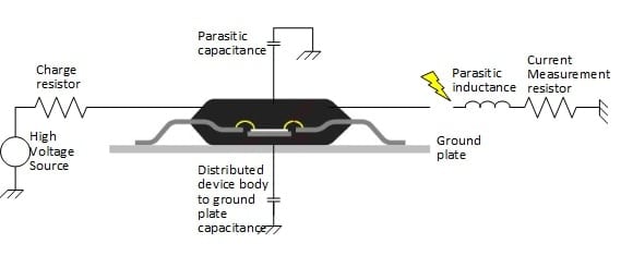
A standard CDM ESD test will measure the characteristics of the waveforms when an external ground touches the DUT pin of the device which is charged. This buildup is then discharged from the device and into the ground. While the device is kept in a position, the discharge will be measured, and the effect recorded.
CDM are higher and stronger than HBM discharges because there are no inherent limits. So, the testing will reveal any vulnerabilities of the electronic device to this form of discharge.


