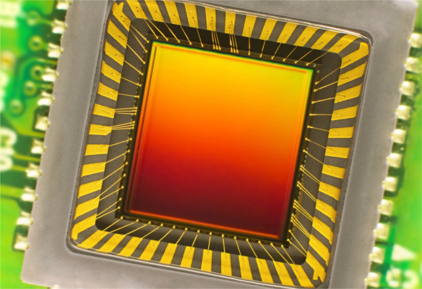
Imagine a world where every moment is captured with immaculate clarity, from the delicate hues of a sunset to the swift action of a sporting event. The heart of this imagery revolution lies in the CMOS image sensor (CIS), a masterpiece of technology little known outside expert circles. Its evolution has been pivotal in the development of digital imaging.
The CMOS (Complementary Metal-Oxide-Semiconductor) image sensor’s tale began not so long ago, yet it revolutionized cameras and imaging in a blink. Understanding its mechanics, how it transforms photons into pixels, is to comprehend the poetry of modern technology.
In this ultimate guide, we delve into the CMOS image sensor’s intricate world, exploring its advantages over its predecessors, its wide-ranging applications, and the future developments that promise to further enhance our visual experiences. Join us on a journey into the pixel depths where innovation meets the eye.
CMOS Image Sensor Market and Industry
CIS revenues stagnated in 2022, achieving $21.3B, in the continuity of a soft-landing situation compared to the largely inflated growth experienced in previous years. The general inflation in 2022 translated to significant slowdown in consumer products sales such as smartphones (-10%). However, higher-end CIS products and new sensing opportunities will sustain the mobile CIS market in the coming years. Automotive cameras are experiencing a large growth enabled by in-cabin, viewing, and ADAS applications, promoted further by safety regulations. The share of the mobile CIS market should continue to decrease with respect to the growing share of automotive, security, and industrial CIS, with the resulting product mix maintaining the overall ASP beyond $3. We have adjusted downward our long-term CIS forecast, with a 5.1% revenue CAGR from 2022 – 2028, and the resulting CIS revenues should reach $29B by 2028. (source: Yole Group)

History of CMOS Image Sensor
The genesis of CMOS (Complementary Metal Oxide Semiconductor) image sensor technology can be traced back to the early 1960s, with the inception of complementary metal-oxide-semiconductor fabrication techniques. This served as the foundation for subsequent advances in semiconductor devices. However, it was not until the late 20th century that CMOS image sensors began to emerge as a viable alternative to their established counterpart, the CCD (Charge-Coupled Device) sensors.
The initial iterations of CMOS sensors had limitations, particularly in the areas of image noise and sensitivity. The early 1990s marked the pivotal period when the concept of an active pixel sensor (APS) was introduced by scientists Eric Fossum and his team at the NASA’s Jet Propulsion Laboratory. The Active Pixel Sensor with intra-pixel charge transfer was an innovative breakthrough that significantly enhanced image quality, effectively catalyzing the evolution of modern CMOS image sensor technology. The transition from passive to active pixel sensors allowed for on-chip amplification, dramatically improving the dynamic range and noise ratio.
By the end of the 1990s, CMOS sensors started to show a substantial reduction in power consumption, thereby overtaking the more power-hungry CCD sensors in battery-operated devices like digital cameras. This progressive shift was supported by advancements in manufacturing that allowed for larger pixel sizes and thus, better image quality. As the new millennium unfolded, the proliferation of CMOS technology was marked by its adoption not just in consumer electronics but also in a wide range of applications, extending to industrial, medical, and automotive sectors.
Overview of CMOS Image Sensor technology
The CMOS image sensor operates on the principle of converting an optical image into an electronic signal. At the core of the CMOS sensor lies an array of pixels, each constituted by a photodetector and an individual readout circuit. The photons striking the sensor’s surface generate electrical charge within these photodetectors, which is subsequently transformed into a voltage signal by the active amplification circuitry.
One of the distinguishing elements of a CMOS sensor is its architecture that allows for the integration of several key functions, such as analog-to-digital conversion and various signal processing functions, directly onto the chip. This integration considerably enhances its efficiency and the rate at which images can be read and processed, known as frame rates, thus enabling high-speed photography and video capture.
Furthermore, the scalability of CMOS technology facilitates the design of sensors with exceptionally high image resolution, as a direct consequence of reducing pixel size without compromising on the performance or increasing power supply demands exponentially. This has led to the emergence of CMOS sensors boasting gigapixel capabilities.
To complement their light sensitivity and color accuracy, CMOS sensors often employ a color filter array (CFA), which interpolates the color information for each pixel to produce a full-color image. The dynamic range of the CMOS sensors also ensures that they can capture details across a wide range of exposure conditions, from shadows to highlights, thus catering to a plethora of imaging applications.
Another hallmark that sets CMOS sensors apart is their flexibility regarding shutter sensors. They can operate using either a global shutter, capturing the entire frame simultaneously, or a rolling shutter, which reads out the image row-by-row. Each method has its unique advantages and applications, with the global shutter being especially prevalent in high-speed or industrial scenarios to avoid distortion, and the rolling shutter offering a more compact and less costly option for many consumer-grade cameras.
In conclusion, CMOS image sensor technology has firmly established itself as a powerhouse within the realm of digital imaging, driven by its low power consumption, high image resolution, and ability to provide a broad dynamic range. The wide range of applications it addresses underscores its versatility, while the continued innovation within the sector promises further enhancements for this cornerstone of modern digital imaging.
Working Principle
The fundamental working principle of CMOS (Complementary Metal Oxide Semiconductor) image sensors hinges on the photoelectric effect, where photon absorption by the semiconductor material results in the liberation of charge carriers—electrons and holes. Structurally, a CMOS sensor is an intricate matrix of individual photodetectors, known as pixels, embedded into a substrate of silicon. Each pixel incorporates a photo-sensitive region and several transistors, forming an integrated circuit capable of both detecting light and readout functionality.
Upon illumination, each pixel’s photo-sensitive region accumulates an electric charge commensurate to the intensity of light incident upon it. The photogenerated charge, bearing a direct relationship to the light’s intensity, is temporarily stored in the pixel’s potential well, which is effectively a charge storage site.
Subsequent to the accumulation phase, the active pixel sensor architecture enables the conversion of this stored charge into a voltage by the embedded transistors. These amplifying transistors within the pixel execute an on-the-spot amplification of the signal before it is routed to the chip’s periphery. This local amplification attribute is a principal differentiator from CCD sensors, wherein charge transfer precedes voltage conversion.
The conversion process does not culminate here; the voltage signals must transmogrify into digital data comprehensible to digital devices. Consequently, CMOS sensors are typically supplemented with onboard analog-to-digital converters (ADCs), which discretize the amplified voltage into a binary form, thereby rendering a pixel’s charge as a digital value. Each pixel’s data, an ensemble of binary digits, encapsulates the intensity and gradation information necessary for image reconstruction.
Additionally, CMOS technology permits the integration of other signal processing functions directly on the sensor chip. Logic circuits deployed for functions like noise reduction, exposure control, and color space conversion result in enhanced image fidelity while facilitating rapid throughput and versatility in various imaging applications.
The CMOS sensor’s capacity to execute these processes in situ—charge accumulation, signal amplification, analog-to-digital conversion, and additional processing—underpins its remarkable speed and power efficiency, distinguishing it as the preferred choice for high-performance imaging applications.
How CMOS Image Sensor captures and converts light into digital signals
The acquisition and translation of optical information into digital signals by a CMOS image sensor encompass a sophisticated sequence of events that entails photodetection, charge-to-voltage conversion, and subsequent digitization.
- Photodetection: Upon light entering the camera lens, it passes through a color filter array (CFA), frequently a Bayer filter, which imparts color specificity to respective pixels. In each pixel, the photo-sensitive element accumulates electric charge proportionate to the intensity and wavelength of incident photons.
- Charge-to-Voltage Conversion: The accumulated charge in each pixel’s potential well is read by the pixel’s own active components, which convert the electric charge into a voltage signal. This localized charge-to-voltage conversion process mitigates readout noise and preserves signal integrity, as the signal degradation associated with longer readout paths is circumvented.
- Analog-to-Digital Conversion (ADC): The analog voltage signal is relayed to the ADC integrated onto the sensor chip or situated in close proximity. The ADC samples the analog signal, assigning a discrete digital value that corresponds to the signal’s amplitude.
- Signal Processing: Post conversion, the raw digital data may undergo additional processing via on-chip digital processors. This processing could involve noise reduction algorithms, white balance correction, and demosaicing, wherein the digital data from the CFA is interpolated to produce accurately colored pixels for the final image.
- Output Generation: The processed digital signals are then sent as image data to the camera’s central processing unit (CPU) or directly to an output interface, culminating as pixels on a display or as digital files for storage and further manipulation.
It is worthwhile to depict this process in a tabular form to elucidate the signal flow:
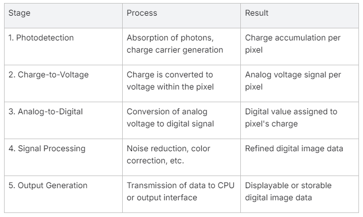
By traversing this articulated pathway, a CMOS image sensor adeptly translates the ephemeral play of light and color into a static tableau of digits, enabling the digital representation of our vibrant reality.
Advantages of CMOS Image Sensor over CCD Sensors
CMOS (Complementary Metal Oxide Semiconductor) image sensors have emerged as a dominant technology in the realm of semiconductor devices, eclipsing the popularity of traditional Charge-Coupled Device (CCD) sensors in many imaging applications. This preeminence is attributed to several inherent advantages that CMOS technology brings to the table, chiefly revolving around power efficiency, system integration, operational speed, and noise performance.
To intelligently assess the superiority of CMOS sensors over their CCD counterparts, it’s essential to delineate specific areas of comparison:
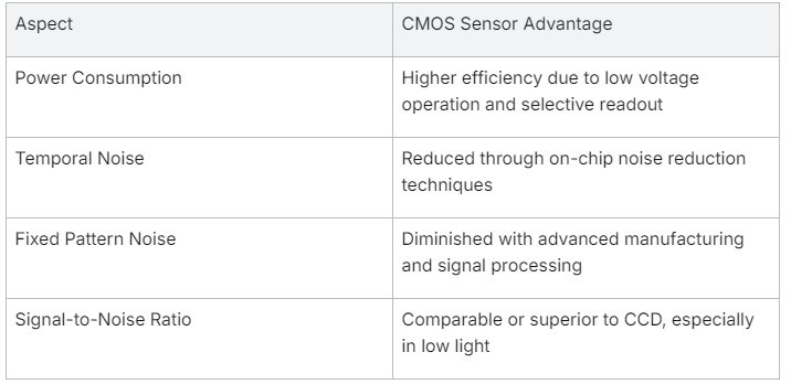
Lower Power Consumption and Reduced Noise Levels
CMOS sensors significantly outperform CCDs in terms of power consumption. CCD sensors require a high-voltage power supply for the charge transfer process, leading to greater power usage. Conversely, CMOS sensors operate at lower voltages and only activate specific portions of the chip during the readout process, which translates to enhanced power efficiency.
In terms of noise, the advancements in CMOS technology have allowed for remarkable reductions in both temporal noise and fixed pattern noise through on-chip noise reduction techniques and the parallel processing of signals. Modern CMOS sensors thus achieve Signal-to-Noise Ratios (SNR) that render them suitable even in low-light conditions.
Here’s a comparative view encapsulated in a table format:
Higher Frame Rates and Faster Readout
The architecture of CMOS sensors, where each pixel contains its own amplification and readout circuitry, facilitates parallel processing of the pixel signals. This enables swift data transfer and faster frame rates as compared to CCDs, where charge must be sequentially transferred and read at one point. The ability to read out specific regions of interest rather than the entire sensor array (windowing) further expedites the process and enhances the speed of CMOS sensors, making them ideal for applications demanding high-speed imaging and video capture.
Integration of Image Sensor and Processing Circuitry on the Same Chip
A distinguishing feature of CMOS image sensors is the potential for high levels of integration. CMOS technology allows for the assimilation of various circuit functions, including the ADC and image processing algorithms, directly onto the sensor chip. This integration confers several benefits, including compact design, reduced system complexity, and enhanced reliability due to the minimization of interconnects. By co-locating processing elements on the same substrate, CMOS sensors demonstrate a marked advantage over CCD sensors, which often require off-chip components to perform analogous functions.
The integration prowess of CMOS sensors is depicted in the list below:
- On-chip Analog-to-Digital Conversion (ADC)
- On-chip timing and control circuitry
- Integrated signal conditioning (e.g., Correlated Double Sampling (CDS) for noise reduction)
- Embedded processors for complex algorithms (e.g., demosaicing, auto-exposure)
In summary, the tactical architectural decisions underlying CMOS image sensor design endow them with a competitive edge over CCD sensors, categorically in domains where power consumption, noise minimization, operational speed, and system integration are pivotal considerations.
Applications of CMOS Image Sensors
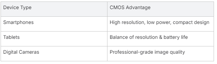
Consumer Electronics: Smartphones, Tablets, and Digital Cameras
CMOS image sensors serve as the cornerstone of digital imaging technology in a plethora of consumer electronics. Smartphones, tablets, and digital cameras exploit these sensors for their superior image resolution, power supply efficiency, and miniaturized form factor. In smartphones, the demand for high-quality digital images has propelled the development of advanced CMOS sensors with larger pixel sizes and elaborate color filter arrays, thus expanding the dynamic range and color fidelity. Digital cameras reap the benefits of wide-range CMOS sensors with substantial pixel counts, enabling professional-grade image resolution. Tablet devices, which require moderate resolution but prioritize long battery life, integrate CMOS sensors to balance image quality with power consumption.
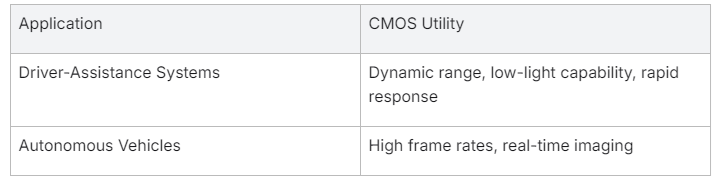
Automotive Industry: Driver-Assistance Systems and Autonomous Vehicles
The automotive industry increasingly favors CMOS image sensors for their rapid exposure time and the ability to function optimally across a range of lighting conditions. Driver-assistance systems utilize CMOS sensors for critical functions like lane departure warnings and collision avoidance. Such systems demand low-light performance and robust dynamic range to ensure driver and vehicular safety. In the burgeoning field of autonomous vehicles, CMOS sensors are integral to providing real-time data essential for decision-making algorithms, where temporal resolution and minimal shutter lag are crucial.
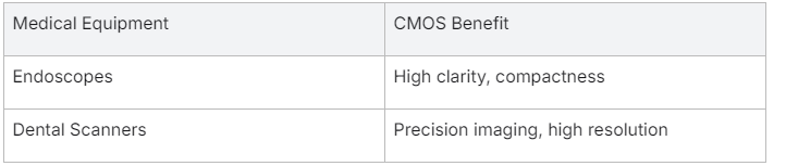
Medical Imaging: Endoscopes and Dental Scanners
Medical imaging heavily depends on CMOS sensors due to their ability to offer high-quality images while maintaining compactness and efficiency within medical instruments. Endoscopes, designed for minimally invasive procedures, employ CMOS sensors to transmit vivid and detailed images from within the body, aiding in accurate diagnostics and surgical interventions. Dental scanners benefit from the small pixel size and high resolution of CMOS sensors to create precise and clear imaging, crucial for diagnoses and treatment planning, which are essential in modern dental care practices.
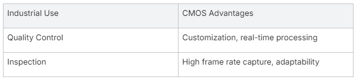
Industrial Machine Vision: Quality Control and Inspection
In industrial applications, machine vision systems integrate CMOS image sensors to facilitate meticulous quality control and inspection processes. The active pixel sensor architecture of CMOS technology enables industrial cameras to capture images at high frame rates and process these images in near real-time, essential for automating production lines and ensuring product quality. The versatility of CMOS sensors allows for customization to meet specific industrial needs, such as varying exposure times and sensitivity levels.
In each application domain, CMOS image sensors deliver a blend of performance features tailored to the needs of the environment, marked by their exceptional versatility, energy efficiency, and superior imaging capabilities. Their range of applications echoes their adaptability and innovation within the field of semiconductor devices.
CMOS Image Sensor Technologies
Complementary Metal Oxide Semiconductor (CMOS) image sensor technology has revolutionized the way we capture and process images. This class of semiconductor devices leverages the potential of active pixel sensor (APS) architectures to provide superior image quality with low power consumption. By converting incoming photons into electrical charge, these sensors are able to produce digital images with impressive dynamic range and fidelity. CMOS sensors are further distinguished by their on-chip integration capabilities, offering built-in analog-to-digital converters (ADCs) and readout electronics that streamline the image acquisition process.
The architectural advancements in CMOS sensors have significantly reduced the Noise Ratio, contributing to greater sensitivity and reduced power draw. Moreover, the ability to operate at varying frame rates and exposure times underscores the versatility of CMOS sensors across a vast range of applications, from industrial machine vision to medical imaging. The incorporation of advanced color filter arrays atop individual pixels allows for accurate color reproduction, complementing the sensor’s spatial resolution and sensitivity thresholds.
With the ongoing miniaturization of semiconductor devices, CMOS sensors continue to evolve, achieving larger pixels within limited spaces while enhancing their functionality through sophisticated on-chip electronic readout circuits. Advances such as backside illumination (BSI) have further propelled the performance, enabling these sensors to collect more light and thereby improving low-light performance. As CMOS technology matures, it remains central to innovations in digital imaging, driving forward an array of applications that demand high-quality visual data.
Active Pixel Sensor (APS) Structures
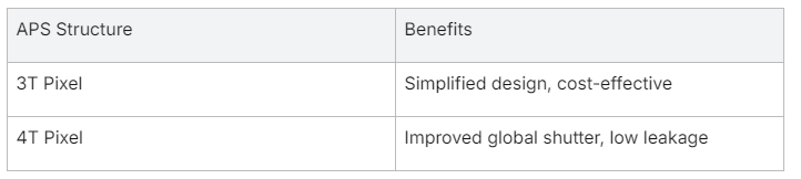
Within the CMOS sensor ecosystem, the active pixel sensor (APS) structures have become the norm due to their varied and intrinsic advantages. In an APS, each pixel contains a photodetector and an active amplifier which leads to an increase in signal-to-noise ratio as well as reduced image lag. The APS architecture allows for enhanced on-chip functionalities including noise correction and non-destructive readouts. The APS design comprises several transistors; the most common being the three-transistor (3T) pixel, although advanced structures like the four-transistor (4T) pixel are widely adopted to provide global shutter capabilities and further suppress dark current.
Modern CMOS image sensors may also implement pinned photodiode (PPD) technology within the APS. PPDs offer lower dark current, facilitating a higher dynamic range and improved image quality, especially in environments with broad illumination ranges. The APS technology allows each pixel to work independently, which enables faster readout speeds—a critical aspect for high frame rate applications in both consumer electronics and specialized industrial imaging tasks.
Analog-to-Digital Converters and Readout Electronics
The use of analog-to-digital converters (ADCs) is a critical aspect of CMOS sensor functionality. ADCs transform the analog electrical charge accumulated by the photodiodes into digital signals that can be further processed and stored. The integration of ADCs directly onto the CMOS sensor chip enables parallel processing, which reduces readout time and enhances the speed at which the sensor can operate. There are various forms of ADC architectures, such as successive approximation register (SAR), pipeline, and sigma-delta, each with its own advantages in terms of power consumption, speed, resolution, and circuit complexity.
CMOS sensors typically include readout electronics, which manage tasks like amplification, noise reduction, and initial signal processing. These elements are integral to shaping the quality of the final image as they impact parameters like the sensor’s dynamic range and sensitivity. The readout circuitry in CMOS sensors not only handles the transfer of charge from the sensor’s pixels but also sequences the operations of the ADCs, enabling complex imaging functions to be executed efficiently.
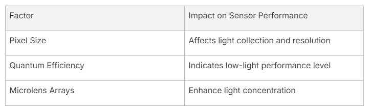
Spatial Resolution and Sensitivity Threshold
The spatial resolution of a CMOS sensor is determined by its pixel size and the total number of pixels. Larger pixels can capture more photons, leading to enhanced sensitivity, a crucial factor for low-light conditions. Sensors with smaller pixels, while enabling higher spatial resolution, might suffer reduced sensitivity due to less photon collection area per pixel, resulting in a compromise between resolution and light-collection efficiency.
The sensitivity threshold, conversely, is dependent on the sensor’s quantum efficiency and the design of the photodetector elements. It denotes the lowest light level at which the sensor can still produce a quantifiable image. Moreover, technologies such as microlens arrays are employed to concentrate light into the photodiodes, boosting the sensitivity of the sensor and mitigating inefficiencies due to pixel scaling.
The balance between spatial resolution and sensitivity is a critical consideration in sensor design, governing the range of potential applications. High-resolution sensors with smaller pixels are often selected for applications needing fine detail, such as surveillance or scientific imaging, while sensors with larger pixels and greater sensitivity are more suitable for low-light photography and astronomical applications. Thus, CMOS sensor technology continues to evolve with a fine-tuned balance between these two parameters to meet the specialized needs of various imaging scenarios.
Image Quality and Performance
The robustness of an imaging system is widely gauged by its image quality and performance metrics, directly tied to the prowess of its CMOS image sensor. Superior image quality, which encompasses sharpness, noise levels, and color accuracy, underpins the sensor’s ability to accurately represent the visual environment. Similarly, performance is evaluated by assessing how well the sensor adapts to varying light conditions, motion, and other environmental factors.
Factors affecting image quality, such as noise reduction and dynamic range
Image quality is significantly influenced by a sensor’s ability to reduce noise and maintain a high dynamic range. Noise in digital imagery, manifesting as random speckles, can detract from image clarity and is often amplified in low-light conditions. CMOS sensors reduce noise through multiple strategies, including on-chip noise-correction algorithms and cooling systems to minimize thermal noise.
The dynamic range of a sensor defines its capacity to capture the lightest and darkest areas of a scene without losing detail. A wider dynamic range allows for more information to be recorded and rendered in the final image. CMOS image sensors (CIS) exploit various techniques to heighten dynamic range, such as multiple exposure HDR or integrating wider bit-depth ADCs that can discern subtler gradations of brightness.
Sensitivity to light and accurate color reproduction
A sensor’s sensitivity to light is paramount for capturing usable images in diverse lighting scenarios. Highly sensitive CMOS sensors boast greater quantum efficiency, which translates to a higher proportion of incident photons being converted to electrons. The implementation of advanced technologies, like backside illumination, bolsters light sensitivity even further by reducing the amount of circuitry that can block incoming photons.
Accurate color reproduction is a non-trivial challenge that image sensors must surmount, attained through a meticulously calibrated color filter array and precise post-processing algorithms. Each pixel within the CMOS sensor is typically covered by a filter—red, green, or blue—to simulate the human eye’s response to different wavelengths of light. The sensor’s ability to balance these color inputs directly impacts the vividness and lifelike nature of the captured images.
Impact of pixel size on image resolution
The size of individual pixels within a CMOS image sensor is a double-edged sword that affects image resolution. Larger pixels boast a superior capability to gather light, contributing to enhanced sensitivity and reduced noise, which is irreplaceable in low-light conditions. Conversely, smaller pixels allow for a greater number to be packed onto a sensor, increasing the resolution, which enables sharper images with more detail.
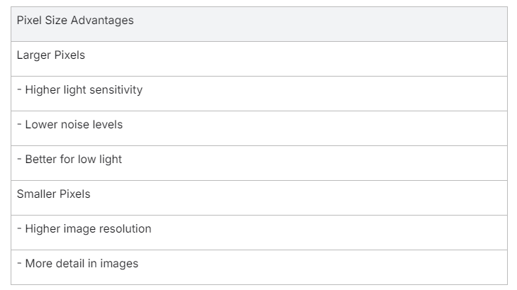
Designing an effective CMOS image sensor, therefore, involves a careful balance between pixel size and the total number of pixels, tailoring the sensor to the specific imaging demands of its intended application, be it in astrophotography with a necessity for sensitivity or in medical imaging where detail resolution is paramount.
Future Developments in CMOS Image Sensor Technology
The relentless pursuit of innovation within the semiconductor industry is driving substantial advancements in CMOS Image Sensor technology. As digital imaging becomes increasingly vital across a spectrum of fields, from consumer electronics to aerospace and biomedicine, there is a strong impetus to evolve sensor capabilities. The quest for refinement hinges on enhancing image performance while managing factors such as power consumption, pixel size, and electrical charge handling to cater to the escalating demands of high-resolution capture and computer vision applications.
Advancements in light sensitivity and noise reduction techniques
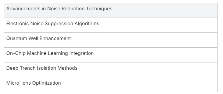
In the vanguard of CMOS sensor development, enhancing light sensitivity and mitigating noise are pivotal to the expansion of their operative envelope. Engineers are exploring novel photodiode architectures and refining silicon substrate treatments to augment quantum efficiency and photon to electron conversion rates. These advancements are crucial to extend the low-light capabilities of image sensors.
Noise reduction is another focal point, where innovations in electronic and quantum well capacities aim to decrease read noise—extending the signal-to-noise ratio envelope. Advances in image processing algorithms and the utilitarian applicability of deep learning can help discern and abate noise patterns in real-time. CMOS sensors with integrated machine learning capabilities are anticipated, which would bolster noise reduction strategies at the sensor-level and in post-capture processing.
Curved sensors for improved optical performance and reduced distortion
The next frontier in sensor architecture is projected to be the integration of curved CMOS sensors. Mirroring the human eye, curved sensors can dramatically diminish optical aberrations, including vignetting and distortion that are intrinsic to flat plane sensing arrays. Such concave designs necessitate flexible electronics and innovative changes to the photolithographic fabrication processes. These curved sensors promise to simplify lens design while amplifying field-of-view sharpness and uniformity.
Curved sensors are poised to revolutionize sectors where bulky lens assemblies were previously requisite, like in security cameras and smartphone optics. They offer a leap in miniaturizing imaging systems whilst concurrently soaring optical performance.
Integration of CMOS Image Sensors with other cutting-edge technologies
The future of CMOS image sensors is deeply entwined with their integration alongside a multitude of cutting-edge technologies. Advanced material science plays a role where we see the incorporation of graphene or black silicon layers to further sensitivity in the IR and UV spectrums, creating vast new use cases in fields such as night-vision, medical and astro-imaging.
On the computational front, the synergy of CMOS sensors with on-chip processing units powered by AI and machine vision algorithms facilitates smarter, more autonomous data acquisition and analysis. The burgeoning IoT paradigm is fostering a need for sensor integrations capable of in-situ imaging analytics, impacting home automation, industrial monitoring, and automotive systems. Semiconductor devices incorporating CMOS sensors will not only have to capture images but also comprehend and interact with their environment.
Additionally, developments in 3D stacking and chip-scale packaging technology enable a drastic reduction in power consumption and footprints of CMOS sensors, making them integral to wearable and mobile applications where space and energy efficiency are vital.
In the tableau of technological progress, CMOS image sensor advancements stand prominent, presaging a future where their application transcends conventional boundaries to invigorate a wider spectrum of industries.
Wafer Stitching
Wafer stitching is a critical process in the manufacturing of image sensors. This process involves aligning and bonding individual sensor dies that have been cut from silicon wafers into a larger sensor array. By stitching together multiple sensor dies, manufacturers can create larger image sensors with higher resolutions. This is important because the larger the sensor die size, the lower the number of sensors per wafer, which can lead to higher costs. Wafer stitching allows for more efficient use of the silicon wafer, maximizing the number of sensors that can be produced from a single wafer.
Precision cutting and alignment of the sensor dies during the stitching process are essential to avoid defects and ensure that each sensor in the array functions properly. By carefully stitching together the sensor dies, manufacturers can create seamless sensor arrays that deliver high-quality images with accurate color reproduction and high sensitivity to light. Overall, wafer stitching is a key step in the production of image sensors that are used in various imaging devices, from smartphones to professional cameras.
Foundries Providing CMOS Image Sensor


 Partner with us