Introduction
In the semiconductor industry, where the integration of cutting-edge technologies defines the next generation of electronics, Sofics is recognized for its innovation and reliability. With a portfolio that has empowered over 130 companies worldwide, Sofics’ IP solutions have become synonymous with performance, robustness, and efficiency.
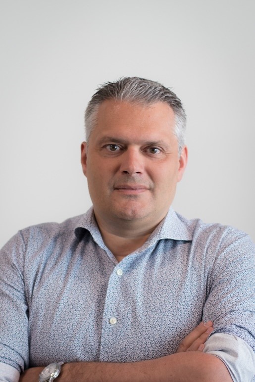
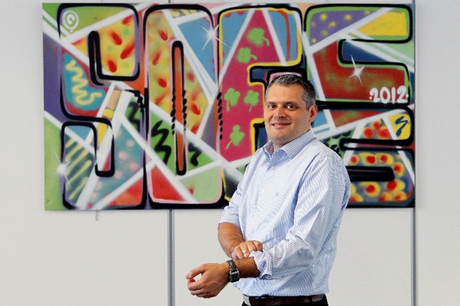
At the heart of Sofics’ technological advancement is Olivier Marichal, Chief Engineering, leading a team of 15+ engineers. With a career spanning over two decades, Olivier’s journey from a fresh graduate to a leading expert in ESD protection and unique I/O circuits has been marked by innovation, research, and a commitment to excellence.
Today, we sit down with Olivier to delve into the details of IC design, explore the challenges and opportunities in the industry, and understand how Sofics is setting new standards in semiconductor IP.
Olivier, could you tell us about your early days at Sofics, how your journey began?
Joining the team at Sofics, or Sarnoff Europe as it was known back in 2004, was the start of my career. It was a much smaller team then, composed of brilliant minds and passionate individuals. Koen, our CEO, had a vision that was contagious, and Henk was paving the way in business development. Engineers like Bart, Benjamin, Frederic, Geert, Gerd, Markus and Pieter created a dynamic and innovative environment. Being part of such a dedicated team was truly inspiring.
At that time, we were deeply involved in projects with all of the leading semiconductor companies in Japan, a country known for its cutting-edge technology and high quality standards in the semiconductor industry. My role primarily involved creating ESD protection devices tailored for the process technology in the IDM fabs of these companies. This was a challenging but incredibly rewarding task, as it allowed us to push the boundaries of what was possible with ESD protection at the time, especially in advanced SOI, CMOS and BCD technologies that are now all considered mature, like the 130nm, 90nm, 65 and 40nm CMOS processes.
The opportunity to travel frequently to Japan and participate in the yearly EOS/ESD Symposium in various USA locations was another aspect of the job that I thoroughly enjoyed. It not only allowed me to connect with industry leaders and peers from around the world but also helped me follow the latest trends and advancements in our field. Those early days at Sofics were formative and exhilarating, setting the stage for the innovative work we continue to do today.
Tell us about Sofics
From our inception to date, we’ve supported more than 130 companies globally, empowering them to achieve higher performance, robustness, and efficiency in their IC designs. Our technology has been characterized on 11 foundries, including advanced nodes at TSMC, UMC, GF, and Samsung Foundry, demonstrating our flexibility and the trust these industry leaders place in our solutions.

One of the key benefits of working with Sofics is our ability to safeguard the core of ICs across a broad spectrum of applications. Our IP is instrumental in 40% of recent Bluetooth products, billions of smartphone imager chips, over a billion FPGA chips, and is a used in numerous automotive and data center applications. This wide adoption underscores our IP’s versatility and reliability.
Our solutions cater to specific needs that go beyond the capabilities of standard foundry I/O pads. For example, our custom cells provide higher ESD robustness for critical interfaces like DisplayPort, HDMI, USB, and automotive applications. We also offer lower parasitic capacitance for high-speed interfaces. Moreover, we enable significantly reduced design time and costs. Our solutions achieve up to 100x lower leakage for wireless or sensor interfaces, offering unparalleled efficiency.
Flexibility is another cornerstone of our offerings. In scenarios where there is a need for fail-safe, hot-swap, cold-spare interface requirements, Sofics delivers custom solutions that meet these specialized demands without compromise.
The cornerstone of our success lies not just in our technological prowess but in our commitment to adding value to our clients’ projects. By partnering with Sofics, IC designers gain access to gold-standard solutions that enable peace of mind knowing their designs are protected by the best in the business.
You recently celebrated your 20-year anniversary at Sofics. What changed for you and Sofics in those 2 decades.
When I started, I was one of the engineers deeply involved in the technical aspects of our projects. My focus was developing state-of-the-art ESD protection solutions and delivering those to customers. Over the years, my role expanded significantly. When the team expanded, we decided to create 2 management roles. One person was responsible for the commercial projects while I was asked to lead the R&D efforts. At Sofics we spend a lot of our time (easily 50% or more) on new developments to make sure our technology is silicon proven on the newest processes before customers need it. Today, I lead the entire engineering team, overseeing not just the R&D projects but also the customer-oriented operations. This shift from a purely technical role to a leadership position that encompasses both R&D and customer projects has been both challenging and rewarding.
For Sofics, the evolution has been equally transformative. In our early years, our deliverables were primarily the layout of innovative ESD clamps. These solutions were then integrated into I/O libraries and PHYs by our IDM customers. Our customers could focus on developing their own novel interface circuits while relying on us for the crucial aspects of ESD protection. However, as the semiconductor landscape shifted towards a more fabless model, our customers’ expectations evolved too. They began seeking more comprehensive solutions, prompting us to expand our offerings beyond ESD clamp layouts to include analog I/Os or complete libraries that come with openaccess schematics, models, and more.
Our evolution didn’t stop there. Recognizing the need for circuits that could handle higher voltages, we embarked on developing unique functional I/O circuits. These circuits, designed to enable higher voltage tolerance, such as 3.3V in 1.8V processes, marked a significant milestone in our journey. We began delivering not only the ESD protection but also the functional receiver/transmitter circuits. For our LIN transceiver / PHY this also included ensuring EMC and ESD protection are both covered.
Looking back at these two decades, the change has been profound. From the technological advancements we’ve embraced to the broadening of our offerings, each step has been a leap towards meeting and exceeding the evolving needs of the semiconductor industry. My journey from being ‘one of the engineers’ to leading Sofics’ engineering team has been intertwined with the company’s growth, a testament to our shared vision and relentless pursuit of excellence.
What aspects do you like at Sofics?
One of the most attractive aspects of working at Sofics is the opportunity to engage with cutting-edge technology and technologists on a daily basis. Over the years, we have always validated our IP across the most advanced process nodes available. From our initial collaborations with top IDM companies in Japan like Toshiba to our work with leading fabless companies such as Altera, and now, our cherished partnerships with the largest foundries in the industry. It’s incredibly fulfilling to see our IP implemented on the latest commercially available FinFET and GAAFET nodes, advanced BCD processes, and most relevant SOI processes. This not only keeps us at the forefront of the semiconductor field but also pushes us to continually advance our skill and capabilities.
Equally inspiring is the diversity of our engineering team. We have bright minds from across the globe, as well our local region, Flanders, each bringing their unique perspectives and insights into semiconductor physics. This diversity fuels our creativity and innovation, making Sofics not just a workplace but a thriving hub of ideas and solutions that challenge the status quo.
Moreover, the complexity of the challenges presented by our customers never ceases to amaze me. We frequently encounter requirements that push the boundaries of what’s possible in terms of reducing leakage, capacitance, and IP area usage, or extending the voltage range. These challenges keep our work interesting and ensure that no two days are the same. They drive us to keep learning and adapting, ensuring that we are always ready to meet our clients’ needs with innovative and efficient solutions.
In summary, it’s the access to leading-edge process technology, the privilege of working with great people, and the continual engagement with challenging and interesting problems that make working at Sofics a truly rewarding experience
What do you do outside work hours?
Outside of my professional life, I cherish the time spent with my family. I’m married, and have two wonderful teenage daughters who bring a lot of joy and energy into our lives. We share a love for nature and take trips that allow us to escape the hustle of daily life and reconnect with the environment. Some of our recent memorable trips include a picturesque drive through the Breton countryside and exploring the majestic fjords of Norway last year.
When I find some quiet time for myself, I indulge in a few personal passions that keep me balanced. One of them is enjoying a occasional sip of fine whisky—an interest that offers a pleasant diversion from the day-to-day. I also take piano lessons, which has been a fun challenge.
Reading is another passion of mine, particularly historical books. Delving into history allows to learn from the past and gain perspectives that enrich one’s understanding of the world. It’s fascinating to draw parallels between historical events and the present day.


 Partner with us