

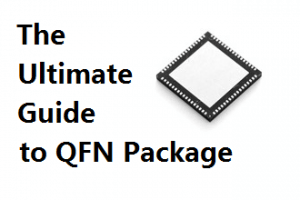
QFN Package Overview
The QFN (Quad Flat No-lead) package is probably the most popular semiconductor package today because of four reasons: low cost, small form factor and good electrical and thermal performance. In this article we will provide an overview to QFN packaging, discuss QFN package technical details and

As semiconductor industry continues on its path to improve its productivity and profitability, the industry faces roadblocks due to huge capital investments with poor RoI. For past few decades ITRS has provided guidance to the research community and associated funding agencies worldwide, in setting up technological challenges and driving progress
Read More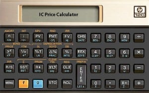
The IC Price Calculator is based on a standard price model that consists of all the required steps in IC manufacturing:
Wafer Price
Assembly/Package Price
Test Price
Yield
The IC Price Calculator is very easy to use and provides quick price estimate of IC price.
Read More
Cisco Systems has acquired semiconductor company Leaba Semiconductor for $350-$400 million. Leaba was established in 2014 and operates in stealth mode.
According to Leaba’s website “Leaba is a fabless semiconductor company providing innovative solutions for significant infrastructure challenges. Leaba is backed by blue-chip investors and led by seasoned entrepreneurs

The leading nanoelectronics research center, imec, and digital research and incubation center, iMinds, today announced that its respective board of directors have approved the intention to merge the research centers. Using the imec name, the combined entities will create a world-class, high-tech research center for the digital economy. The transaction
Read More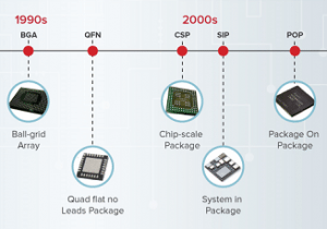
Since the invention of the first semiconductor package in 1965, the semiconductor packaging technology has grown dramatically and several thousands of different semiconductor package types have been made. The chart below presents the semiconductor packaging history. Particularly it shows the two major trends in semiconductor packaging: addressing high pin