


Last week’s post was addressed primarily to those of you who are already designing SoCs. We made the point that more and more SoCs have multiple processors, either homogenous or heterogeneous, and that most or all of those processors do or will have caches. This led to the main conclusions of the
Read More
Gordon Moore said‚ on the 40th anniversary of his law that “Moore’s law is really about economics.” What did he really mean by that? In 1965 when Gordon Moore put forth Moore’s law based on his observation, those years were Golden years of Free Market Capitalism in America. The entire decade
Read More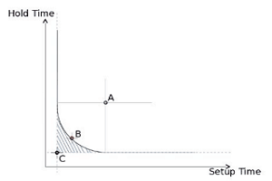
This is a guest post by Dolphin Integration which provides IP core, EDA tool and ASIC/SoC design service.

This is a guest post by Methodics that delivers state-of-the-art semiconductor data management (DM) for analog, digital and SoC design teams.
The topic of IP quality in the SoC era is difficult to define, and solutions to problems relating to IP quality, verification, and use are hard to find. Debates rage between IP users, suppliers,
Read More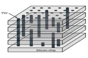
“The long term growth of the equipment & materials business will be supported by the expansion of 3D TSV stack platforms” says Yole (Yole Développement) in its latest report, “Equipment & Materials for 3DIC & WLP Applications“. The market research and strategy consulting company, Yole proposes a deep analysis of the equipment &
Read More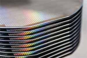
SEMICON West 2014 in San Francisco was a great place to meet bloggers in the semiconductor industry to get updated on the status of 450mm diameter silicon wafers. On one side, there is a good news about the unprecedented level of collaboration taking place between the design and construction professionals
Read More