


HOD HASHARON, Israel and BLOOMINGTON, Minnesota, U.S. – November 8, 2022 – Weebit Nano Limited (ASX:WBT), a leading developer of next-generation memory technologies for the global semiconductor industry, and SkyWater Technology (NASDAQ: SKYT), the trusted technology realisation partner, announce the first silicon wafers integrating Weebit’s embedded Resistive Random-Access Memory (ReRAM) module
Read More
TEMPE, Ariz. — October 24, 2022 — Amkor Technology, Inc. (Nasdaq: AMKR), a leading provider of semiconductor packaging and test services, today announced its commitment to supporting European initiatives to achieve strategic regionalization for automotive semiconductors.
The proliferation of applications for automotive semiconductors continues to accelerate — from electrification,

Cesson-Sévigné (France) — November 3rd, 2022 – Secure-IC, the rising leader, and the unique global provider of end-to-end cybersecurity solutions for embedded systems and connected objects, announces today the acquisition of Silex Insight’s security business. Silex Insight is a leading provider for flexible and scalable security IP cores solutions which perfectly
Read More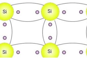
In this article we will discuss extrinsic semiconductors. In short extrinsic semiconductors are devices that have been doped with specific chemicals. This process helps modifying the electrical properties of a relatively pure semiconductor crystal.
Intrinsic (pure semiconductor) or un-doped semiconductors have free electrons and holes. Both of them are

This interview was held with Racheli Ganot, Founder and CEO of Ready Group (formerly Rachip).
Tell me about Ready?
Ready Group (formerly Rachip) is an R&D 360 Firm, experts in end-to-end chip development, SW and HW for the semiconductor and high-tech industries. Ready Group teams have been
Hyderabad, India and Santa Clara, USA – Oct 17, 2022 – MosChip Technologies, a Semiconductor and Embedded system design services company, today announced that the company has joined the Design Center Alliance (DCA) of TSMC Open Innovation Platform® (OIP). The TSMC DCA focuses on chip-implementation services and system-level design solutions to help lower
Read More