


The corner-based timing signoff approach is a historical and traditional method that has justified a development and enhancements of conventional STA tools and signoff flows. The number of signoff corners exponentially grows along with an increase of variation sources, their magnitude, and timing margins. It becomes a bottleneck in
Read More
During the last decades, important advances in microelectronic techniques and technologies had been fueling the introduction of new wireless enabled products accessible to a large number of people around the world. Without the competitive price offered by CMOS, the widespread use of wireless enabled engineering complex devices, e.g. smartphones, tablets, etc. would certainly have been delayed.
Read More
The corner-based timing signoff approach is a historical and traditional method that has justified a development and enhancements of conventional STA tools and signoff flows. The number of signoff corners exponentially grows along with an increase of variation sources, their magnitude, and timing margins. It becomes a bottleneck in the
Read More
There has been a substantial amount of discussion about the noise of power supplies and its harmful effect inside wireless electronic devices such as cell phones and WiFi or bluetooth enabled portable devices. Due to an increased pressure to extend battery life in portable devices, switching (or DC-DC) regulators have
Read More
For decades, electronics product innovation has been incremental in nature, relying largely on the next generation of semiconductors to deliver performance improvement. For almost 50 years Moore’s Law has delivered 2x performance (power or cost) improvement in semiconductors every 18 months, outpacing any product or system level innovation cycle that
Read More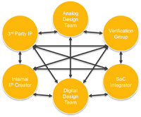
hat comes to mind when you hear the term IP Distribution? How do people like ARM and MIPS get their cores into people’s hands? Pricing, contracts and legal issues? Maybe third-party Web sites like Chip Estimate and Design & Reuse? Yes, they are all factors in how independently developed IP
Read More