
IC Insights will release its May Update to the 2019 McClean Report later this month. This Updateincludes a discussion of the 1Q19 IC industry market results, a detailed quarterly IC market forecast for the remainder of this year, and a look at the top-25 1Q19 semiconductor suppliers.
Over its 60-year history, the IC industry is
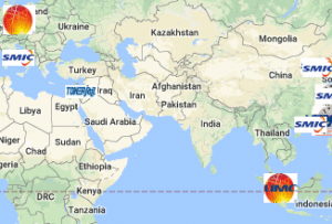
IC Insights recently released its new Global Wafer Capacity 2019-2023 report that provides in-depth detail, analyses, and forecasts for IC industry capacity by wafer size, process geometry, region, and product type through 2023. Figure 1 shows the world’s installed monthly wafer production capacity by geographic region (or country) as of December
Read More
Lekha Wireless, the leading wireless communications and embedded systems technology company, has signed an agreement with T2M, the world’s largest independent global semiconductor IP provider, to act as a global representative and business development partner of Lekha Wireless’ IP and technology solutions.
Lekha Wireless has a wide range of

Amkor Technology announced today it has partnered with Mentor to release Amkor’s SmartPackage™ Package Assembly Design Kit (PADK), the first in the industry to support Mentor’s High-Density Advanced Packaging (HDAP) design process and tools. Amkor’s award-winning High-Density Fan Out(HDFO) process can now be used in conjunction with Mentor’s software to deliver
Read More
HDL Design House, provider of digital, analog, and back-end design and verification services and products in numerous areas of SoC, will host a joint technical workshop with Mentor, a Siemens business, at the Aviation Electronics Europe conference on June 19th, 2018 at the MOC Event Center in Munich, at 4pm.
Read More
Energy management is at the heart of the new generation of systems-on-chips (SoCs) targeting battery-powered applications. More complex power architectures are required to enable devices to run on the same battery for years rather than months. These new architectures often result in new noise challenges.
To deal with the