


[November 11, 2024] – Taiwan Semiconductor Manufacturing Company (TSMC), the world’s leading contract chipmaker, announced today it is suspending production of advanced artificial intelligence (AI) chips for Chinese customers, effective Monday. This action follows a U.S. Department of Commerce directive to halt shipments of advanced chips to Chinese companies, pending
Read More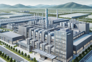
[November 8, 2024] – Semiconductor Manufacturing International Corporation (SMIC), China’s leading semiconductor foundry, today announced its financial results for the third quarter of 2024, reporting record-breaking revenue of US$2.17 billion. This represents a 14% sequential increase and a 34% year-over-year surge, marking the first time the company has exceeded the
Read More
The third quarter of 2024 painted a mixed picture for the foundry industry, with some vendors celebrating profits while others grappled with losses. This highlights the diverse landscape of this crucial sector of the semiconductor world.
Samsung:
Overall Q3 2024 Sales: 79.1 trillion won ($57.4 billion) – Up
Read More
November 5, 2024 — GlobalFoundries, the world’s third-largest semiconductor foundry, has been fined $500,000 by the U.S. Bureau of Industry and Security (BIS) for unauthorized shipments of chips to SJ Semiconductor, an affiliate of the blacklisted Chinese chipmaker SMIC. The fine follows a Reuters report detailing 74 unlicensed shipments valued
Read More
DALLAS and AIZU, Japan, Oct. 24, 2024 /PRNewswire/ — Texas Instruments (TI) (Nasdaq: TXN) today announced it has begun production of gallium nitride (GaN)-based power semiconductors at its factory in Aizu, Japan. Coupled with its existing GaN manufacturing in Dallas, Texas, TI will now internally manufacture four times more GaN-based
Read More
Executive Summary
In Q3 2024, X-FAB reported revenues of USD 206.4 million, marking a 12% decline year-on-year but a slight increase of 1% quarter-on-quarter. The company’s bookings amounted to USD 217.1 million, resulting in a book-to-bill ratio of 1.05, reflecting a robust demand despite market challenges. EBITDA was reported at