


[September 4, 2023] – Semiconductor Manufacturing International Corporation (SMIC), China’s leading chipmaker, has significantly reduced its capital expenditures (capex) in the first half of 2024, despite a surge in semiconductor equipment spending by China overall.
SMIC’s H1 capex dropped from $12 billion in H1 2023 to $8 billion in H1

Sep. 2, 2024 —- TrendForce’s latest investigations have found that the arrival of China’s 618 mid-year shopping season as well as inventory levels of consumer electronics reaching healthier levels, have prompted customers to begin restocking components, resulting in urgent orders for wafer foundries. This surge in demand has significantly improved capacity
Read More
Aug-27th 2024, the Biden-Harris Administration announced that the Department of Commerce and HP Inc. have signed a non-binding preliminary memorandum of terms (PMT) to provide up to $50 million in proposed direct funding under the CHIPS and Science Act. The proposed funding would support the expansion and modernization of HP’s
Read More
The global foundry industry’s revenue grew about 9% QoQ and 23% YoY in Q2 2024, according to Counterpoint Research’s Foundry Quarterly Tracker. The sequential growth was mainly driven by strong AI demand. CoWoS supply remained tight, with potential upsides in capacity expansions focusing on CoWoS-L going forward. Despite slower demand
Read More
United Microelectronics Corp (UMC), Taiwan’s second-largest pure-play wafer foundry, marked a milestone yesterday with the arrival of the first equipment tools for its Phase 3 expansion at Fab12i in Singapore. The ceremony was attended by representatives from the Singapore Economic Development Board (EDB), Jurong Town Council (JTC), the Institute of
Read More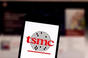
Taipei, August 16 – Taiwan Semiconductor Manufacturing Co. (TSMC), the world’s largest contract chipmaker, has announced the purchase of a plant and equipment from flat panel maker Innolux Corp. for NT$17.14 billion (US$531 million). The acquisition, located in the Southern Taiwan Science Park, encompasses a 317,445 square meter facility and related
Read More