

Multi Project Wafer (MPW) emerged in the 1970’s to help companies and researchers prototype their silicon and demonstrate their work. It was the early days of the semiconductor industry when firms like Fairchild, IBM and others were applying technology innovation to create smaller, faster and cheaper chips. Back then, Multi-Project
Read More
The world’s largest contract chip maker, Taiwan Semiconductor Manufacturing Co (TSMC), is being expected to secure more than half of all of Apple’s new mobile chip in 2016. This is due to their better production roadmap planning. They’re expecting that since the Taiwanese manufacturer has a clear roadmap for their
Read More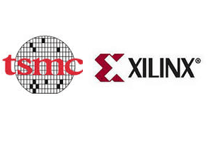
The war between TSMC and Samsung is heating up and it’s expected to last well throughout the decade. The war only got hotter when TSMC announced that they will begin producing 7nm processors in 2017. Xilinx will be their very first customer.
Xilinx Inc. made the announcement late yesterday that
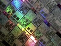
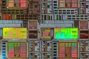
Semiconductor wafer is absolutely invisible in our daily life but it exists in a form of an ASIC or an IC in each and every electronic device we use. Semiconductor wafer is a round piece of silicon which consists of silicon dies that are designed to perform a very specific
Read More
The 14nm technology development between Samsung and GlobalFoundries that started last year is now reaching its final step by releasing the availability schedule of the process technology including the 2 main flavors.
The primary concept of the strategic collaboration is to make 14nm FinFET technology available at

During the last decades, important advances in microelectronic techniques and technologies had been fueling the introduction of new wireless enabled products accessible to a large number of people around the world. Without the competitive price offered by CMOS, the widespread use of wireless enabled engineering complex devices, e.g. smartphones, tablets, etc. would certainly have been delayed.
Read More