

Get the semiconductor daily news directly to you by subscribing to our email list. For ASIC designer and managers, staying updated with the latest news, technologies, and trends is crucial. Here are the lastest news from the semiconductor industry.
With an impressive 20% growth in MEMS revenue compared to 2013, and sales revenues of more than $1.2B, Robert Bosch GmbH is the clear #1. From Yole Développement’s yearly analysis of “TOP 100 MEMS Players”, analysts have released the “2014 TOP 20 MEMS Players Ranking”. This ranking shows the clear
Read More
Getting funding for a semiconductor startup is not getting easier. According to CBIngishts, there have been fewer than 20 Angel/Seed and Series A deals in the USA in each year since 2009.
So where is all the funding channeled to? In 2013, close to a quarter of all VC

The corner-based timing signoff approach is a historical and traditional method that has justified a development and enhancements of conventional STA tools and signoff flows. The number of signoff corners exponentially grows along with an increase of variation sources, their magnitude, and timing margins. It becomes a bottleneck in
Read More
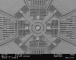
During the last decades, important advances in microelectronic techniques and technologies had been fueling the introduction of new wireless enabled products accessible to a large number of people around the world. Without the competitive price offered by CMOS, the widespread use of wireless enabled engineering complex devices, e.g. smartphones, tablets, etc. would certainly have been delayed.
Read More
Bob Colwell, Director of the Microsystems Technology Office (MTO) at the Defense Advanced Research Projects Agency (DARPA), recently made a compelling statement about the end of Moore’s Law: “When Moore’s Law ends, it will be economics that stops it, not physics. Follow the money.”
If we move beyond Moore’s

The corner-based timing signoff approach is a historical and traditional method that has justified a development and enhancements of conventional STA tools and signoff flows. The number of signoff corners exponentially grows along with an increase of variation sources, their magnitude, and timing margins. It becomes a bottleneck in the
Read More
There has been a substantial amount of discussion about the noise of power supplies and its harmful effect inside wireless electronic devices such as cell phones and WiFi or bluetooth enabled portable devices. Due to an increased pressure to extend battery life in portable devices, switching (or DC-DC) regulators have
Read More
For decades, electronics product innovation has been incremental in nature, relying largely on the next generation of semiconductors to deliver performance improvement. For almost 50 years Moore’s Law has delivered 2x performance (power or cost) improvement in semiconductors every 18 months, outpacing any product or system level innovation cycle that
Read More
As technologies advance, the semiconductor industry and its traditional business model face a myriad of ongoing complexities demanding an ever accelerating state of operational agility. The electronics and healthcare markets are experiencing unprecedented change through mass market consumerization and global adoption. For most chip companies, gone are the days of
Read More
Over the last 5 years lead generation has fundamentally changed. Companies used to participate in expensive events and focus mostly on branding activities. But today potential customers have direct access to all the products information they need, things are different.
In other industries, marketing & sales teams understand that their