



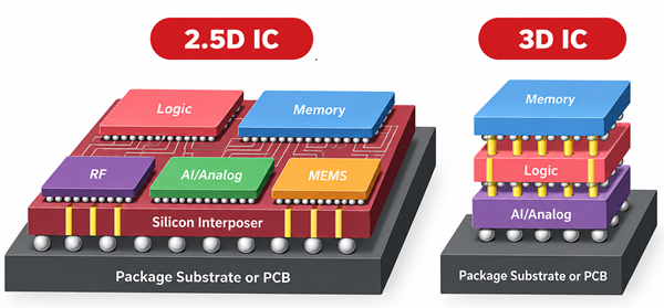
As chipmakers move from monolithic SoCs toward chiplets, high-bandwidth memory (HBM) and heterogeneous integration, the interposer has become one of the most important components inside an advanced package. The interposer sits between dies or chiplets and the package substrate, providing far denser routing than a conventional PCB or package substrate can normally achieve.
The choice of interposer material influences routing density, electrical performance, package size, thermal behavior, coefficient of thermal expansion (CTE), manufacturing cost and ultimately whether a multi-die package can be produced economically.
| Interposer Type | Best For | Main Advantage | Main Limitation |
|---|---|---|---|
| Silicon | AI accelerators, HPC, HBM, high-density chiplets | Highest proven routing density and mature fine-pitch integration | Large silicon area and TSV processing make it expensive |
| Organic / RDL | Large packages, cost-sensitive multi-die systems, moderate-to-high density | Lower cost potential, flexible build-up structure and easier package scaling | Cannot match silicon at the finest routing geometries |
| Glass | Future very-large AI/HPC packages and next-generation substrates/interposers | Dimensional stability, electrical isolation and attractive large-format potential | Manufacturing ecosystem and high-volume production are still developing |
What Does an Interposer Do?
An interposer is an intermediate routing structure placed between semiconductor dies and the package substrate. In a typical 2.5D package, logic chiplets, HBM stacks or other dies are mounted on the interposer using microbumps or similar fine-pitch interconnects. The interposer then connects downward to the package substrate through larger bumps.
This creates a hierarchy of interconnect density:
- On-die metal: the finest dimensions.
- Interposer: extremely dense package-level routing between dies.
- Package substrate: coarser routing between the interposer and package balls.
- PCB: the coarsest level of system routing.
The reason this hierarchy matters is bandwidth. A conventional organic package substrate can become impractically large when thousands of signals must be routed between multiple dies. Fine-pitch interposer routing keeps connections short and enables much wider interfaces than would be practical at PCB level.
Shorter links can also reduce signal loss and the energy required to drive each connection. This is one reason interposer-based packaging has become closely associated with HBM, AI accelerators and large chiplet architectures.
Why Interposer Material Matters
An interposer is not simply a mechanical spacer. It must route many high-speed signals while maintaining signal integrity, power integrity, thermal reliability and dimensional stability. The interposer material therefore affects several important design parameters.
| Design Factor | Why It Matters |
|---|---|
| Routing density | Determines how many die-to-die signals can be routed in a given area. |
| CTE | CTE mismatch between die, interposer and package substrate creates mechanical stress during thermal cycling. |
| Electrical isolation | Affects parasitics, crosstalk and signal integrity. |
| Thermal conductivity | Influences how heat moves through a densely integrated package. |
| Via technology | TSVs, TGVs or organic vias determine how signals and power move vertically through the interposer. |
| Manufacturing format | Wafer size, panel size and lithography limits affect maximum package size and cost. |
| Cost per area | Large AI and HPC packages may require interposers several times the area of a conventional die. |
Silicon Interposers
Silicon is the most established material for very high-density interposers. Its major advantage is simple: interposer wiring can be manufactured using semiconductor-style lithography and metal processing, enabling much finer features than conventional organic package substrates.
A passive silicon interposer does not use transistors. It is effectively a large piece of processed silicon containing multiple metal-routing layers, vertical vias and landing pads. Because it is fabricated in a semiconductor fab, the routing density can approach dimensions that are impossible with ordinary PCB manufacturing.
Advantages of Silicon Interposers
- Very fine metal line and spacing.
- High microbump density.
- Excellent fit for HBM and wide die-to-die interfaces.
- Short high-speed interconnects.
- Well-established manufacturing ecosystem.
- Silicon-to-silicon CTE matching can simplify some thermo-mechanical challenges.
- TSVs can provide vertical power, ground and signal connections.
- Silicon can also support future active-interposer concepts because it is a semiconductor.
Silicon interposers do not usually require a leading-edge logic process. Mature process technology is sufficient because the interposer primarily contains metal routing rather than dense transistor logic. However, the interposer can still be expensive because it is physically large and processed using wafer-fab equipment.
The Silicon Interposer Cost Problem
For an advanced package, the interposer must normally be large enough to accommodate all of the dies mounted on top of it. As AI processors increase in size and add more HBM stacks, the interposer can become substantially larger than an ordinary chip.
The economics are therefore very different from those of a small silicon die. Even if the silicon interposer uses a much older process node, a large amount of wafer area is still consumed. Additional metal layers and TSVs further increase cost.
There is also a lithography issue. Very large interposers can exceed the normal reticle exposure area, requiring multiple exposures to be stitched together. This adds manufacturing complexity and places greater emphasis on alignment and yield.
Silicon Interposers in Production in 2026
Silicon is not merely a research option. It is already used at large scale in production advanced-packaging platforms. TSMC states that its CoWoS-S platform uses a large silicon interposer for high-density integration of logic chiplets and HBM and currently supports silicon interposers up to roughly 3.3 times reticle size, or about 2,700 mm². TSMC positions CoWoS-S specifically for ultra-high-performance computing applications.
This production maturity is a major reason silicon remains the reference solution when the design requires the highest interconnect density and the project can absorb the packaging cost.
Organic Interposers and RDL Interposers
Organic interposers are an attempt to capture many of the system benefits of silicon interposers without paying for a large piece of processed silicon.
They are conceptually related to high-density package substrates. Multiple layers of dielectric and copper are built up to create the routing structure. The manufacturing techniques can resemble advanced substrate processing, although the dimensions required for an interposer are typically much tighter than those of an ordinary PCB.
The fundamental tradeoff is that organic materials cannot normally achieve the same line-and-space density as semiconductor-fabricated silicon. But many packages do not need the absolute maximum density everywhere.
Advantages of Organic Interposers
- Lower potential cost than a large silicon interposer.
- Large package sizes can be economically attractive.
- Build-up construction allows multiple routing layers.
- Mechanical compliance can help absorb CTE mismatch.
- Suitable for many chiplet packages that do not require the finest possible routing.
- Strong compatibility with existing package-substrate and OSAT manufacturing ecosystems.
Limitations of Organic Interposers
- Coarser routing geometry than silicon.
- Lower maximum local interconnect density.
- More challenging for extremely wide die-to-die buses.
- Material properties and CTE must be carefully modeled.
- High-density designs can still require expensive advanced build-up processes.
Organic Interposers in Production in 2026
Organic/RDL interposers have moved well beyond the experimental stage. TSMC’s CoWoS-R uses a redistribution-layer interposer built from polymer and copper and has been in volume production since 2023. TSMC specifies a minimum routing pitch of 4 µm, corresponding to approximately 2 µm line width and 2 µm spacing.
TSMC also uses RDL-based structures in CoWoS-L, which combines a molding-based interposer with high-density local silicon interconnect chips. This hybrid approach is important because it demonstrates that future packages do not necessarily have to choose between “all silicon” and “all organic.” Dense silicon can be placed only where it is required, while a lower-cost RDL structure handles the rest of the package.
Glass Interposers
Glass has attracted increasing attention because it offers a different set of mechanical and electrical properties from both silicon and organic laminates.
Glass is an electrical insulator, which can provide attractive signal-isolation characteristics. Its composition can also be engineered to tune properties such as thermal expansion. In addition, glass can potentially be manufactured in large wafer or panel formats, an important advantage as AI and HPC packages grow beyond traditional reticle-size boundaries.
Vertical connections through glass are typically made with through-glass vias (TGVs), which serve a role analogous to TSVs in silicon.
Potential Advantages of Glass
- Excellent electrical insulation.
- Potentially strong dimensional stability.
- Attractive flatness for very large packages.
- Large wafer and panel manufacturing possibilities.
- Tunable material properties through glass composition.
- Potential for high-density TGV-based routing.
- Interesting long-term path for large AI and HPC packages.
Challenges of Glass
- TGV formation and metallization remain challenging at advanced densities.
- Handling and mechanical reliability require specialized processes.
- Supply chains and design rules are less mature than for silicon and organic substrates.
- High-volume manufacturing is not yet as broadly established as silicon interposer production.
- Design-tool and assembly ecosystems are still evolving.
What Changed by 2026? Glass Is Moving Closer to Commercial Use
The 2025 technical literature still characterized glass interposers as largely a research-stage technology. During 2026, however, industry activity accelerated substantially.
In July 2026, Intel and Lens Technology announced a strategic collaboration focused on glass substrate-based advanced packaging for future AI, data-center and specialized-compute platforms. Intel says the collaboration is intended to explore higher interconnect density, better performance and improved power efficiency using advanced glass processing.
Intel’s 2026 packaging research program also includes dedicated work on glass-core substrates for AI and HPC, indicating that glass is moving from basic material research toward a more complete packaging platform.
TSMC’s direction is also important. According to TrendForce in June 2026, TSMC is developing panel-based advanced packaging and is expected to move toward glass-core substrates over the longer term, although commercial-scale glass-core production is still expected later than its current silicon and organic packaging technologies.
Silicon vs Organic vs Glass: Detailed Comparison
| Attribute | Silicon Interposer | Organic / RDL Interposer | Glass Interposer / Glass-Core Direction |
|---|---|---|---|
| Routing density | Highest and most mature | Moderate to high | Potentially high; still evolving |
| Electrical isolation | Good with proper design | Good | Potentially excellent due to insulating glass |
| Vertical vias | TSVs | Organic vias / microvias | TGVs |
| Large-area scalability | Limited by wafer economics and reticle stitching | Strong | Potentially very strong |
| Relative cost | Highest for large-area passive structures | Generally lower | Uncertain until broad HVM is established |
| Manufacturing maturity | High | High and increasing | Developing |
| Mechanical compliance | Low | Higher | Material-dependent; attractive dimensional stability |
| Active circuitry possible | Yes, in principle | No conventional transistor integration | Not inherently semiconductor-active |
| Best current fit | Highest-density HBM and chiplet integration | Cost-sensitive and very large heterogeneous packages | Future large-format AI/HPC packaging |
Which Interposer Should You Choose?
Choose Silicon When:
- The package requires the highest available die-to-die routing density.
- HBM integration is central to the architecture.
- Signal bandwidth and fine-pitch interconnect outweigh package cost.
- A proven high-volume manufacturing flow is required today.
- Large numbers of local chiplet connections must fit into a compact area.
Choose Organic / RDL When:
- Cost is a major constraint.
- The package is physically large.
- The design does not need silicon-class routing density across the entire package.
- Mechanical compliance is valuable.
- A hybrid architecture can use local silicon only where very fine routing is needed.
Evaluate Glass When:
- The product roadmap extends into next-generation AI/HPC package sizes.
- Large-area dimensional stability is important.
- The project can tolerate technology-development risk.
- Future TGV density and large-format manufacturing could materially improve the design.
- The packaging supplier already has a defined glass development roadmap.
Application Comparison
| Application | Likely Preferred Direction | Reason |
|---|---|---|
| AI accelerator + multiple HBM stacks | Silicon or hybrid silicon/RDL | Very high bandwidth and extremely dense memory interfaces. |
| Large HPC multi-chiplet package | Silicon, RDL, or hybrid | Depends on how much of the package requires ultra-dense local routing. |
| Cost-sensitive chiplet SoC | Organic / RDL | Can reduce the amount of expensive silicon used for routing. |
| Very large future AI package | Glass worth evaluating | Large-format stability and future interconnect scaling may become attractive. |
| HBM-intensive product entering production now | Silicon | Most established high-density production ecosystem. |
| Package requiring local ultra-dense chiplet links but large overall footprint | Hybrid RDL + local silicon bridge/interconnect | Fine silicon routing is used only where required. |
Interposer Choice Is Becoming a System-Level Decision
Advanced packaging has made the old sequential design model — design the chip first and hand it to a package engineer later — increasingly impractical.
Interposer material affects signal integrity, power integrity, parasitics, routing topology, thermomechanical stress and heat flow. Those factors influence chiplet placement, bump maps, HBM location, power delivery and even the maximum clock frequency that the silicon can reliably sustain.
For this reason, chip, interposer and package development increasingly need to proceed as a co-design exercise. Engineers should evaluate:
- Chiplet and HBM placement.
- Die-to-die interface bandwidth.
- Routing density requirements.
- TSV, TGV or microvia strategy.
- Power and ground distribution.
- Signal integrity and package parasitics.
- CTE mismatch and warpage.
- Thermal coupling between dies.
- Assembly and test strategy.
- Package cost and manufacturing yield.
The Longer-Term Direction: Hybrid Packaging Rather Than One Winning Material
It is tempting to ask whether glass or organic materials will eventually “replace” silicon interposers. The more likely outcome is that the advanced-packaging market will use multiple materials simultaneously.
The highest-density connection regions may continue to use silicon because semiconductor lithography provides exceptional routing density. Larger regions that do not require those dimensions can use RDL or organic materials to reduce cost. Glass may become increasingly important as packages grow and the industry needs flatter, more dimensionally stable large-format structures.
This mixed-material direction is already visible in production architectures that use RDL interposers together with local silicon interconnect structures. The economics are compelling: use expensive fine-pitch silicon only where it creates real system value.
Final Takeaway
Silicon remains the benchmark for advanced interposer performance in 2026, particularly for HBM and high-density AI/HPC packages. Organic and RDL interposers offer an increasingly attractive alternative when package size and cost are dominant considerations. Glass has the potential to become a major platform for the next generation of very large packages, but it should currently be treated as a strategic roadmap technology rather than the automatic choice for near-term high-volume production.
For engineering teams, the right question is therefore not “Which interposer material is best?” but rather: Where does the package need silicon-level routing density, how large must the package become, what reliability constraints apply, and what combination of materials produces the best system-level performance and cost?
Looking for an Interposer or Advanced Packaging Supplier?
AnySilicon can help semiconductor companies connect with packaging, substrate, interposer and assembly providers for BGA, flip-chip, 2.5D, chiplet and other advanced-package projects.
Submit Your Packaging Requirement →
You may also find these AnySilicon resources useful: BGA Packaging Services and BGA Substrate Design.
Sources and Further Reading
- TSMC 3DFabric – CoWoS-S, CoWoS-R and CoWoS-L — current production architectures and interposer options.
- Intel and Lens Technology collaboration on glass substrate-based advanced packaging, July 2026.
- Intel Foundry Packaging & Test Research, 2026 — including glass-core substrate development for AI/HPC.
- TrendForce, June 2026 – TSMC CoPoS and glass-core substrate outlook.