

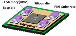
High-bandwidth memory (HBM) is a JEDEC-defined standard, dynamic random access memory (DRAM) technology that uses through-silicon vias (TSVs) to interconnect stacked DRAM die. In its first implementation, it is being integrated with a system-on-chip (SoC) logic die using 2.5D silicon interposer technology.
In June 2015, AMD introduced its Fiji

SK hynix, Inc., Amkor Technology, eSilicon, Northwest Logic and Avery Design Systems have joined forces to offer a complete high-bandwidth memory (HBM) supply chain solution. HBM is a JEDEC-defined standard that utilizes 2.5D technology to interconnect an SoC and an HBM memory stack. Many companies are already using HBM to
Read More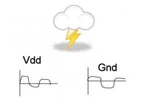
It has been almost two decades since the target impedance concept was first proposed for the design of power distribution networks. Both academia and industry have come a long way since then by proposing solutions for managing power integrity in packages and printed circuit boards (PCB). This paper briefly reviews
Read More
QFN Package Overview
QFN (Quad Flat No-Lead) is a compact surface-mount IC package with electrical contacts located underneath the package instead of protruding leads. QFN packages offer a small PCB footprint, short electrical paths and efficient heat transfer through an exposed thermal pad, making them widely used for RF, analog,
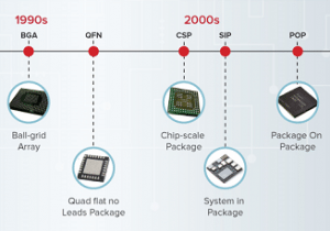
Since the invention of the first semiconductor package in 1965, the semiconductor packaging technology has grown dramatically and several thousands of different semiconductor package types have been made. The chart below presents the semiconductor packaging history. Particularly it shows the two major trends in semiconductor packaging: addressing high pin
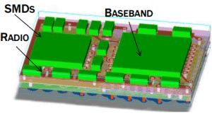
Today, the (SiP) System-in-Package approach offers a new dimension to system integration, far beyond mere dense micro-packaging of existing System on Chip solutions. Not only does SiP offer the capability to integrate almost any kind of companion passive component with a given active circuit, but it also enables flexible combinations
Read More