

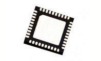
QFN package is probably the most successful package type today. Offering low price, excellent performance and small size, it is an ideal package for many applications.
QFN (quad-flat no-leads) is a plastic SMT package consisting of: a leadframe, single or multiple dies, wirebonds and a molding compound. The
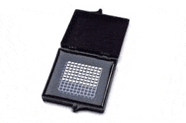
There are many ways to deliver, package and transport silicon products. Here’s a short primer that provides the basic facts regarding how silicon can be packed and delivered to ensure safe transportation with minimum damages.
There are two main options for receiving wafers from your foundry: tested or untested.
Read More
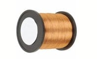
We love copper (Cu) wire. In fact, we already described in our post “Copper Wire (Cu) Reduces Package Cost” the cost advantages of copper wire bonding compared to Gold (Au) wire. Copper wire introduced some challenges to assembly houses (such as ASE, Amkor, STATS ChipPAC) but also offers a few
Read More
Do you know someone that is not eager to reduce their ASIC production costs? I don’t. Some say that redesign changes can lead to significant cost reduction, for instance – using a more advanced silicon technology node to shrink the die size. True, but this is a really big, painful
Read More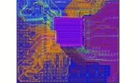
BGA substrate design is a critical step in the development of many ASICs, SoCs, processors, sensors, RF devices and high pin-count integrated circuits. The package substrate acts as the electrical and mechanical bridge between the silicon die and the printed circuit board. It routes signals from the die pads or
Read More
MSL stands for Moisture Sensitivity Level. It represent the amount of time an IC can be exposed to ambient conditions and still be assembled on a PCB without being damaged.
When the antistatic bag is opened and the ICs are exposed to ambient conditions, the moisture in the air
Read More