


Early on in Chip projects, yield is not taken very seriously. The common thinking goes – anyhow there isn’t much to do as this early point of time. However, there are actually several things you can do even before the Chip design starts, which will translate to clear savings.
1-
Read More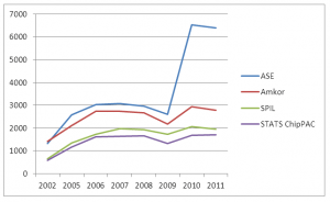
Semiconductor Assembly and Test Services are converting rapidly into a pure outsourcing mode of operation. While today perhaps only 50% of the market is using Outsourced Semiconductor Assembly and Test (OSAT, or SATS) this number is set to increase in the future.
While many of the low-end suppliers are
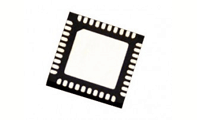
QFN package is probably the most successful package type today. Offering low price, excellent performance and small size, it is an ideal package for many applications.
QFN (quad-flat no-leads) is a plastic SMT package consisting of: a leadframe, single or multiple dies, wirebonds and a molding compound. The
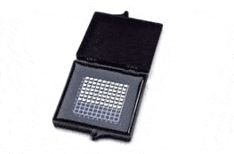
There are many ways to deliver, package and transport silicon products. Here’s a short primer that provides the basic facts regarding how silicon can be packed and delivered to ensure safe transportation with minimum damages.
There are two main options for receiving wafers from your foundry: tested or untested.
Read More
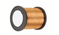
We love copper (Cu) wire. In fact, we already described in our post “Copper Wire (Cu) Reduces Package Cost” the cost advantages of copper wire bonding compared to Gold (Au) wire. Copper wire introduced some challenges to assembly houses (such as ASE, Amkor, STATS ChipPAC) but also offers a few
Read More
Do you know someone that is not eager to reduce their ASIC production costs? I don’t. Some say that redesign changes can lead to significant cost reduction, for instance – using a more advanced silicon technology node to shrink the die size. True, but this is a really big, painful
Read More