

“The long term growth of the equipment & materials business will be supported by the expansion of 3D TSV stack platforms” says Yole (Yole Développement) in its latest report, “Equipment & Materials for 3DIC & WLP Applications“. The market research and strategy consulting company, Yole proposes a deep analysis of the equipment &
Read More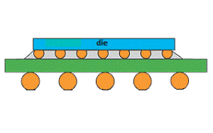
Yole Développement announces its Flip Chip Market and Technology Trends report. Yole Développement’s analysis updates the business status of the Flip-Chip market including data for TIM, underfills, substrates and Flip-Chip bonders. Discover fully updated 2010 – 2018 market forecast, detailed technology roadmap and bottom up approach, plus a strong focus
Read More
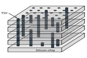
3D Through Silicon Vias (TSV) is in MEMS, CMOS Image Sensors and high-end applications. When will it be used for mainstream consumer applications?… All results are part of the new report released by Yole Développement (Yole): 3DIC & 2.5D TSV Interconnect for Advanced Packaging – 2014 Business Update. This technology
Read More
This is a guest post by Jesse Galloway and Ted Okpe of Amkor Technology. Article reprinted from May 2014 Electronics Cooling magazine.
One of the more challenging thermal resistance measurements to make for electronic packages is the junction-to-case resistance called Theta jc. The equation for Theta jc, equation (1), is straightforward.
Read More
While assembly houses are gradually becoming more and more organized in regards to following internal processes, it seems that we, their customers, are often trying to push them to make shortcuts only because “we are running out of time”.
With chip design cycle time shrinking, production related tasks such
Semiconductor foundries claim they release a new technology node every two years. They may be off by a year or two, but on the whole, this is quite impressive, no doubt. Come to think of it, I don’t believe many of us even change our mobile phone every two years. How
Read More