

Get the semiconductor daily news directly to you by subscribing to our email list. For ASIC designer and managers, staying updated with the latest news, technologies, and trends is crucial. Here are the lastest news from the semiconductor industry.

Launching a hardware startup is difficult. Launching a semiconductor startup is even more complex. Unlike software, where products can be tested, fixed and released quickly, an ASIC project requires careful planning, strong technical execution and the right partners from the very beginning. One mistake in architecture, verification, physical design or
Read More
Sony Semiconductor Solutions and Taiwan Semiconductor Manufacturing Company have signed a non-binding memorandum of understanding to explore a strategic partnership for the development and manufacturing of next-generation CMOS image sensors. Under the proposed structure, the two companies intend to establish a joint venture in Japan, with Sony expected to be
Read More
Semiconductor Design and Verification Services: From Specification to Tape-Out
Developing a semiconductor device requires much more than writing RTL or creating circuit schematics. A successful chip project needs a complete design and verification flow that can reduce risk before tape-out and improve the chance of first-pass silicon success.
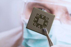
Semiconductor

Semiconductor Manufacturing Cost Breakdown: Wafer, Packaging, Test, Yield and Production Costs
Understanding the semiconductor manufacturing cost breakdown is essential before starting a custom chip, ASIC, or semiconductor production project.
The cost of manufacturing a semiconductor device is not only the wafer price. A complete cost model may include design,

End-to-End ASIC Manufacturing Solutions: From Concept to Production Silicon
Developing a custom ASIC is not only a design project. It is a complete semiconductor supply chain project.
A successful ASIC program requires architecture, circuit design, verification, layout, tape-out, wafer fabrication, packaging, testing, qualification, yield management, logistics, and long-term production

Custom IC Design Firms: How to Find the Right Partner for Your Chip Project
Choosing the right custom IC design firm is one of the most important decisions in a semiconductor project. The right partner can help turn a product idea, system requirement, or existing discrete design into a manufacturable
Custom ASIC Solutions: From Specification to Silicon
Developing a custom ASIC is one of the most important decisions a hardware company can make. A well-designed ASIC can reduce power consumption, improve performance, lower unit cost at volume, protect intellectual property, and create a product advantage that is difficult for competitors

Find Qualified Wafer Dicing Suppliers for Your Semiconductor Project
Wafer dicing is a critical step in semiconductor manufacturing, where processed wafers are separated into individual dies or chips before packaging, assembly, testing or further processing. The dicing process must be accurate, clean and well controlled, as poor dicing can lead
In the world of high-speed SoC design, “almost working” is really just a polite way of saying “an expensive paperweight.”
As we push beyond the 6.4 Gbps threshold with DDR5, the margin for error has essentially disappeared. For engineering leads and decision-makers, the goal is no longer just a

Developing high-performance analog ICs requires deep expertise, precise design methodologies, and strong understanding of process technologies. From power management and sensor interfaces to data converters and high-voltage applications, analog IC design is one of the most specialized areas in semiconductor development.
AnySilicon helps companies connect with experienced analog IC