

Get the semiconductor daily news directly to you by subscribing to our email list. For ASIC designer and managers, staying updated with the latest news, technologies, and trends is crucial. Here are the lastest news from the semiconductor industry.
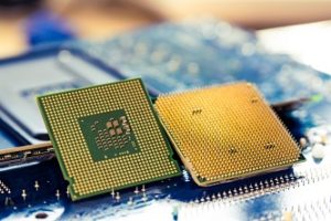
Looking for a BGA packaging company for prototype, low-volume or production semiconductor assembly?
AnySilicon helps semiconductor companies connect with IC packaging and assembly providers offering wire-bond BGA, flip-chip BGA, FCBGA, FBGA and custom substrate-based packaging services worldwide.
Submit your die, substrate, package, ball-count and production-volume requirements and
Looking for a QFN packaging company for prototype, low-volume or production assembly?
AnySilicon helps semiconductor companies connect with IC packaging and assembly providers offering standard and custom QFN packaging services worldwide.
Submit your die, package and volume requirements and AnySilicon can help identify suitable packaging partners for

Finding experienced ASIC verification engineers can be difficult when your chip project requires strong UVM, SystemVerilog, coverage, formal verification, protocol knowledge or complex SoC-level debug.
AnySilicon helps semiconductor companies, startups and engineering teams connect with ASIC verification engineers, UVM specialists, SoC verification experts, formal verification engineers, contractors and
Read More
Finding experienced physical design engineers can be challenging when your ASIC project requires proven expertise in floorplanning, place-and-route, clock-tree synthesis, timing closure, power integrity and signoff.
AnySilicon helps semiconductor companies, startups and engineering teams connect with physical design engineers, RTL-to-GDSII specialists, STA engineers, timing-closure experts, consultants and semiconductor
Finding experienced ASIC design engineers can be difficult when your project requires a specific combination of RTL expertise, SoC integration, low-power design, timing closure, verification awareness and real silicon tape-out experience.
AnySilicon helps semiconductor companies, startups and engineering teams connect with ASIC design engineers, RTL designers, SoC engineers,
Read More
Finding an experienced analog layout designer can be one of the most important steps in a successful analog or mixed-signal IC project. Even a strong schematic can lose performance if the physical implementation introduces excessive parasitics, mismatch, coupling, IR drop or routing asymmetry.
AnySilicon helps semiconductor companies, startups
Read More
Finding experienced analog and mixed-signal IC designers can be difficult, especially when your project requires proven tape-out experience in a specific circuit, process node, foundry or EDA flow.
AnySilicon helps semiconductor companies, startups and engineering teams connect with experienced analog IC designers, mixed-signal engineers, custom layout specialists, contractors
Read More
This interview features Mr. Kazushige Koshika, President of TOPPAN Technical Design Center Inc.
Tell me a bit about your background? How did you first get started with TOPPAN Technical Design Center Inc.?
I had been involved in semiconductor design businesses for many years. Through my previous
Digital isolation is an essential part of many industrial, automotive, energy and power-electronics systems. Digital isolators allow signals to cross an electrical isolation barrier while helping protect low-voltage control electronics from ground-potential differences, high-voltage transients and electrical noise.
Traditionally, engineers have selected digital isolation and isolated interface devices from established

High-voltage DC/DC converters are widely used in industrial electronics, automotive systems, telecommunications, energy storage, battery-powered equipment and other applications where the input supply can be significantly higher than the low-voltage rails required by processors, sensors and control electronics.
Design engineers traditionally source these devices from established analog semiconductor manufacturers. However,