

Because Sondrel offers a full turnkey service of ASIC production from design through to shipping silicon, it knows what is happening with services at every stage of the manufacturing and test process. It says that it has noticed increased lead times for SOC package design and manufacturing, particularly for flip chip BGAs that could impact the overall project timelines.
Ed Loverseed, Sondrel’s Head of Engineering, explained, “People think that they have to do things in a set sequence and hence don’t sort out the bump and ball co-ordinates until the design is finalised and ready to tape out to the fab. Unfortunately, the increased lead times for packaging can now mean that the silicon will be produced before the packaging is ready. This introduces a delay in the whole process so that the devices are not ready for market as predicted.”
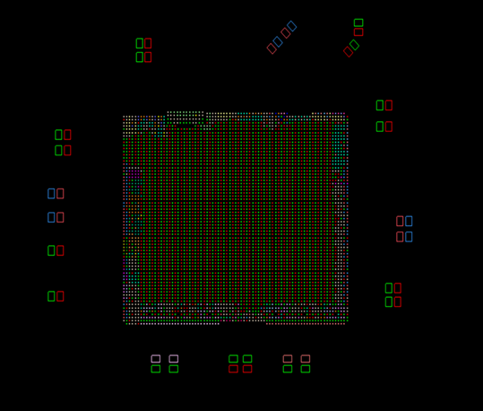
Once it became aware of this issue, Sondrel devised a solution. By assigning die bumps and determining their x/y coordinates relative to the die corner, the SoC package planning and design can be started earlier by generating the bump coordinates before top level physical design and final RDL routing are completed.
Alaa Alani, a principal engineering consultant leading the project explained, “Using the floor plan and the SoC partitions’ locations, the bump locations are determined for each of the macros and PHYs as specified by the IP vendors. For hard macros such as PCIe, HDMI and others, the bumps locations are specified by their relative offset from the macro corner whereas in soft macros (e.g., DDR), it is based on a certain pattern and a minimum pitch used in the bump assignment.”
“The final bump assignment still has to be checked against the final chip layout, but we have found that this method gives an excellent first approximation that is good enough to start the SoC package planning and design,” he added. “As a result, we have eliminated a potential delay and I would advise others to follow this procedure of starting bump layout early.”
About Sondrel™
Founded in 2002, Sondrel is the trusted partner of choice for handling every stage of an IC’s creation. Its award-winning define and design ASIC consulting capability is fully complemented by its turnkey services to transform designs into tested, volume-packaged silicon chips. This single point of contact for the entire supply chain process ensures low risk and faster times to market. Headquartered in the UK, Sondrel supports customers around the world via its offices in China, India, France, Morocco and North America. For more information, visit www.sondrel.com
Press contact:
Nigel Robson, Vortex PR nigel@vortexpr.com +44 1481 233080
Sondrel is a trademark of Sondrel Limited


