

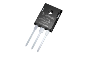
What is a TO-247 Package?
The TO-247 package is a widely used through-hole semiconductor package designed for high-power applications. It is commonly used for devices such as MOSFETs, IGBTs, diodes, and power transistors that require efficient heat dissipation and high current handling.
TO-247 stands for “Transistor Outline 247”, and
TEMPE, Ariz.–(BUSINESS WIRE)–Oct. 6, 2025– Amkor Technology, Inc. (Nasdaq: AMKR), a leading provider of semiconductor packaging and test services, in collaboration with the Trump Administration, today announces the groundbreaking and expanded planned investment of its new state-of-the-art outsourced semiconductor advanced packaging and test campus in Arizona.
The expanded investment includes additional cleanroom space

TEMPE, Ariz. — Aug. 28, 2025 — Amkor Technology, Inc. (Nasdaq: AMKR), a leading provider of semiconductor packaging and test services, today announced revised plans for the location of the company’s new semiconductor advanced packaging and test facility in Arizona.
The facility will be constructed on a 104-acre site within the Peoria
Kaohsiung, Taiwan – August 13, 2025 — ASE Group (Advanced Semiconductor Engineering), the world’s leading OSAT (Outsourced Semiconductor Assembly and Test) provider, has taken a bold step forward in meeting skyrocketing demand for advanced packaging by acquiring a facility from GaAs foundry WIN Semiconductors. The purchase, approved by the board
Read More
Paris, France – May 19, 2025 – Foxconn Technology Group today unveiled a comprehensive €250 million investment plan in Europe, marking a strategic expansion into advanced semiconductor packaging, satellite manufacturing and electric vehicle production on the continent.
Key Highlights:
Joint Venture in Advanced Packaging: Foxconn will form
Read More
May 13, 2025 —- TrendForce’s latest report on the semiconductor packaging and testing (OSAT) sector reveals that the global OSAT industry in 2024 faced dual challenges from accelerating technological advancements and ongoing industry consolidation. While ASE holdings and Amkor maintained leading positions, OSAT providers from China, such as JCET and HT-Tech,
Read More