


Looking for a BGA packaging company for prototype, low-volume or production semiconductor assembly?
AnySilicon helps semiconductor companies connect with IC packaging and assembly providers offering wire-bond BGA, flip-chip BGA, FCBGA, FBGA and custom substrate-based packaging services worldwide.
Submit your die, substrate, package, ball-count and production-volume requirements and
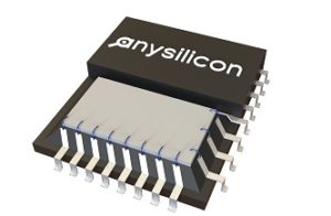
Looking for a QFN packaging company for prototype, low-volume or production assembly?
AnySilicon helps semiconductor companies connect with IC packaging and assembly providers offering standard and custom QFN packaging services worldwide.
Submit your die, package and volume requirements and AnySilicon can help identify suitable packaging partners for

Finding experienced ASIC verification engineers can be difficult when your chip project requires strong UVM, SystemVerilog, coverage, formal verification, protocol knowledge or complex SoC-level debug.
AnySilicon helps semiconductor companies, startups and engineering teams connect with ASIC verification engineers, UVM specialists, SoC verification experts, formal verification engineers, contractors and
Read More
Finding experienced physical design engineers can be challenging when your ASIC project requires proven expertise in floorplanning, place-and-route, clock-tree synthesis, timing closure, power integrity and signoff.
AnySilicon helps semiconductor companies, startups and engineering teams connect with physical design engineers, RTL-to-GDSII specialists, STA engineers, timing-closure experts, consultants and semiconductor
Finding experienced ASIC design engineers can be difficult when your project requires a specific combination of RTL expertise, SoC integration, low-power design, timing closure, verification awareness and real silicon tape-out experience.
AnySilicon helps semiconductor companies, startups and engineering teams connect with ASIC design engineers, RTL designers, SoC engineers,
Read More
Finding an experienced analog layout designer can be one of the most important steps in a successful analog or mixed-signal IC project. Even a strong schematic can lose performance if the physical implementation introduces excessive parasitics, mismatch, coupling, IR drop or routing asymmetry.
AnySilicon helps semiconductor companies, startups
Read More