

An integrated circuit package has the sole purpose of protecting and maintaining one or more integrated circuits. It is usually in the form of a plastic, glass, metal, or ceramic casing which creates a physical barrier of protection against things like impact and corrosion. Furthermore, it helps to hold contact
Read More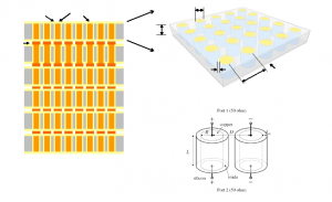
Over the last several years, the buzzword in the electronics industry has been “More than Moore”, referring to the embedding of components into the package substrate and stacking of ICs and packages using wirebond and package on package (POP) technologies. This has led to the development of technologies that can
Read More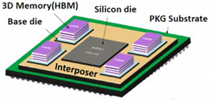
High-bandwidth memory (HBM) is a JEDEC-defined standard, dynamic random access memory (DRAM) technology that uses through-silicon vias (TSVs) to interconnect stacked DRAM die. In its first implementation, it is being integrated with a system-on-chip (SoC) logic die using 2.5D silicon interposer technology.
In June 2015, AMD introduced its Fiji
SK hynix, Inc., Amkor Technology, eSilicon, Northwest Logic and Avery Design Systems have joined forces to offer a complete high-bandwidth memory (HBM) supply chain solution. HBM is a JEDEC-defined standard that utilizes 2.5D technology to interconnect an SoC and an HBM memory stack. Many companies are already using HBM to
Read More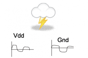
It has been almost two decades since the target impedance concept was first proposed for the design of power distribution networks. Both academia and industry have come a long way since then by proposing solutions for managing power integrity in packages and printed circuit boards (PCB). This paper briefly reviews
Read More
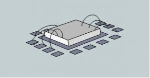
QFN Package Overview
The QFN (Quad Flat No-lead) package is probably the most popular semiconductor package today because of four reasons: low cost, small form factor and good electrical and thermal performance. In this article we will provide an overview to QFN packaging, discuss QFN package technical details and