

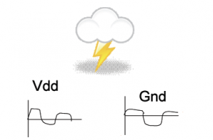
It has been almost two decades since the target impedance concept was first proposed for the design of power distribution networks. Both academia and industry have come a long way since then by proposing solutions for managing power integrity in packages and printed circuit boards (PCB). This paper briefly reviews
Read More
QFN Package Overview
The QFN (Quad Flat No-lead) package is probably the most popular semiconductor package today because of four reasons: low cost, small form factor and good electrical and thermal performance. In this article we will provide an overview to QFN packaging, discuss QFN package technical details and specifications
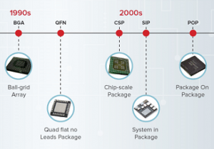
Since the invention of the first semiconductor package in 1965, the semiconductor packaging technology has grown dramatically and several thousands of different semiconductor package types have been made. The chart below presents the semiconductor packaging history. Particularly it shows the two major trends in semiconductor packaging: addressing high pin
Today, the (SiP) System-in-Package approach offers a new dimension to system integration, far beyond mere dense micro-packaging of existing System on Chip solutions. Not only does SiP offer the capability to integrate almost any kind of companion passive component with a given active circuit, but it also enables flexible combinations
Read More
Semiconductor Packaging has become a critical factor to any semiconductor company success. Engineers have to select a semiconductor package effectively to both meet demanding price pressure but also system level performance requirements and size limitations.
Furthermore, with today’s price pressures – companies are spending more time in finding, selecting,
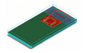
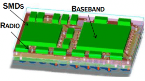
Antenna in Package (or AiP) is an new trend in IC packaging which is an enabler of smaller and high integrated ICs that consists of ICs and Antenna inside a package. Antenna in Package allows integration of all the complex RF components, together with the base-band circuitry into a complete
Read More