

TEMPE, Ariz. and VILA DO CONDE, Porto, Portugal, February 2, 2017 – Amkor Technology, Inc. (Nasdaq: AMKR) and NANIUM S.A. today announced that they have entered into a definitive agreement for Amkor to acquire NANIUM, a world class provider of wafer-level fan-out (WLFO) semiconductor packaging solutions. Terms of the transaction
Read More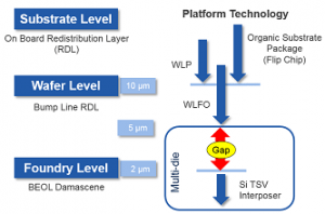
The continued growth of the mobile handset, tablet, and networking markets requires ongoing development of innovative packaging technologies. The required solutions must provide reduced form factor and high thermal and electrical performance as well as increased functional convergence and system integration. To meet the extremely small interconnect feature sizes in
Read More
IC Package Price calculator is an online IC package price estimation tool that covers all the major IC package types exist today.
To use the IC package price tool simply select the IC package type, number of pins and volume and the tool will send you an email with

Qualcomm Incorporated (NASDAQ:QCOM) today announced the opening of Qualcomm Communication Technologies (Shanghai) Co. Ltd., a semiconductor test facility in the Waigaoqiao (WGQ) free-trade zone in Shanghai, and its first foray into providing manufacturing services for semiconductors. By working with Amkor Technology, Inc., one of the world’s leading providers of contract
Read More
Deca Technologies, a wafer level packaging provider to the semiconductor industry, announced today the receipt of an additional $51.5 million investment from a leading electronics company. Combined with the previously announced investment from ASE of $60 million, and following the repurchase of $20.6 million of shares held by Cypress Semiconductor Corp.,
Read More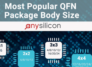
QFN package is the most successful package type today. Offering low price, excellent performance and small size, it is an ideal package for many applications.
QFN package comes in different size and different lead count. This infographics shows the most popular body size and lead count provided by leading OSAT