

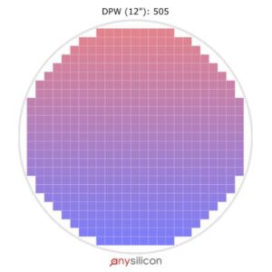
What is a die per wafer calculator?
A die per wafer calculator is a tool used by chip designers and fabs to estimate how many individual dies (aka chips) can be cut from a single semiconductor wafer.
It’s like trying to fit as many square stickers as possible on

Early on in Chip projects, yield is not taken very seriously. The common thinking goes – anyhow there isn’t much to do as this early point of time. However, there are actually several things you can do even before the Chip design starts, which will translate to clear savings.
1-
Read More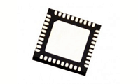
QFN package is probably the most successful package type today. Offering low price, excellent performance and small size, it is an ideal package for many applications.
QFN (quad-flat no-leads) is a plastic SMT package consisting of: a leadframe, single or multiple dies, wirebonds and a molding compound. The
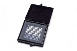
There are many ways to deliver, package and transport silicon products. Here’s a short primer that provides the basic facts regarding how silicon can be packed and delivered to ensure safe transportation with minimum damages.
There are two main options for receiving wafers from your foundry: tested or untested.
Read More

Do you know someone that is not eager to reduce their ASIC production costs? I don’t. Some say that redesign changes can lead to significant cost reduction, for instance – using a more advanced silicon technology node to shrink the die size. True, but this is a really big, painful
Read More
Silicon wafers are the most essential element in the realization of ICs. The semiconductor industry had invested heavily to increase the wafer size during the last 30 years, so while foundries used to produce 1 inch wafers, today’s common wafer size is 300mm (11.8 times larger than 1 inch). There
Read More