

Optimizing ASIC test time is a critical factor in semiconductor manufacturing to enhance efficiency, reduce costs and improve time to market. In this article we will provide strategies you can use and implement in your design to help reduce IC test time. One can consider the following benefits:
Increased Throughput: With the world dealing with chip shortage today, shorter test times allow for higher throughput in production, enabling more chips to be tested and packaged within a given time. This is instrumental for meeting the ever-growing demand for semiconductors in all the sectors by achieving higher manufacturing volumes.
Reduced Costs: IC test time reduction directly impact production costs. Faster testing means lower equipment utilization costs, reduced energy consumption, and less wear and tear on the testing equipment. While testing cost accounted for 2% of the total chip manufacturing cost a few decades ago, it may account for as much as 10% of the total manufacturing cost for newer technologies.
Faster Time-to-Market: Accelerating IC test time can shorten the overall production cycle. This allows manufacturers to deliver new products quicker than their competitors and gain a competitive edge in the market.
Improved Yield Analysis: Faster test time enable quicker feedback on manufacturing defects and issues. This rapid feedback loop allows manufacturers to analyze and address the factors that may be limiting the production yield and make the necessary corrections and adjustments to the design or the manufacturing process in a timely manner.
Scan Testing is a design for test (DFT) technique used to facilitate the detection of various manufacturing faults in the silicon. Scan tests involve capturing data into a set of flop-flops to observe the chip’s behavior. Stuck-at Fault Testing is used to detect manufacturing faults like opens and shorts. The registers of the design are connected in the form of a long shift register, also known as a scan chain. The input patterns are shifted in (Scan Shift), the patterns are then allowed to exercise the combinational logic (Scan Capture) and the captured data is shifted out to be compared against the expected data.
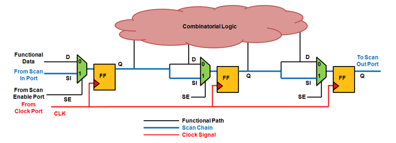
Figure 1: Scan Testing
The test time of the chip is computed as: Time taken to shift in the pattern + 1 capture clock period + time taken to shift the pattern out.
As evident from this equation, scan shift time is the major contributor to the overall scan test time. To cut the scan shift time, the registers are partitioned into multiple scan chains. Theoretically, in an ideal case, designers would cut the length of scan chains to 2 and make the entire operation parallel. However, this approach would entail having a humongous number of scan-in and scan-out ports, which is practically impossible. The achieve a better trade-off between fewer scan-in and scan-out ports and an optimal number of registers in a scan chain, designers use scan compression.
Scan Compression or Embedded Deterministic Test (EDT) involves sending in scan input through a small number of ports. The decompressor logic algorithmically expands the input to generate desired inputs to feed into each scan chain. Once the testing is completed and the capture data needs to be sent out for verification, the data encounters a compressor logic that compresses the bit stream from multiple scan chains to a fewer number of scan-out ports.
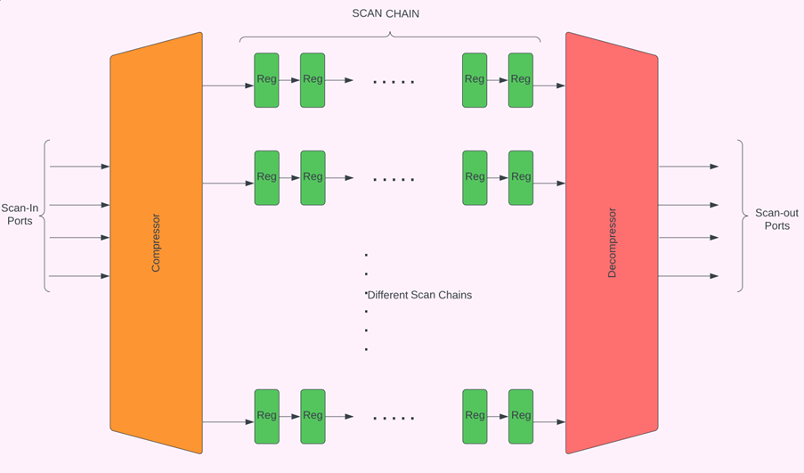
Figure 2: Scan Compression or Embedded Deterministic Test
Another aspect of optimizing the test time is improving the fault coverage. A higher fault coverage would translate into fewer patterns to be exercised on the fabricated chips, thereby reducing test time. DFT techniques rely on the ability to “control” a given node to a desired value, and subsequently on the ability to “observe” the output of a given node to test it against the expected signature. Test point insertion adds registers or combinational logic on deep combinational logic to improve the controllability and observability of the design and achieve the desired fault coverage target with fewer test patterns.
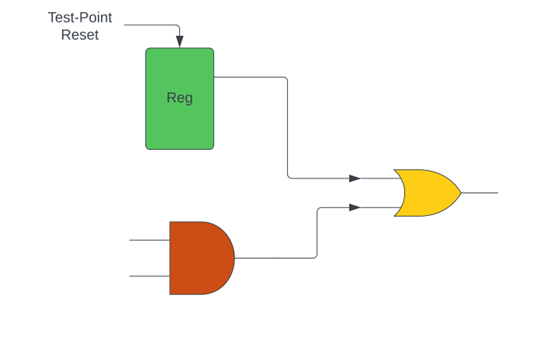
Figure 3: Inserting test-point registers to improve controllability
Inserting registers as test-points typically incurs higher area overhead and minimal timing impact, while inserting combinational logic as test-points usually translates into lower area but some timing impact due to extra RC load observed by the previous stage logic.
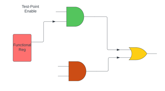
Figure 4: Inserting combinational logic to improve controllability
Designers tend to use the divide and conquer approach when it comes to testing. As an example, when it comes to memory testing, it is quite common for designs to have multiple MBIST controllers. These MBIST controllers test a sub-set of the design memories and may have the option to operate serially or in parallel. Operating more MBIST controllers in parallel cuts down the test time at the cost of increased power dissipation which may result in voltage drop issues on the design.
At the wafer level, parallel testing can be achieved by testing multiple cores on the same chip simultaneously by using multiple test resources.
While parallel testing involves testing different components on the same chip simultaneously, multi-site testing refers to testing multiple chips simultaneously using parallel test equipment. This would need more sophisticated and expensive equipment with increased compute ability, but this can be offset by the cost savings achieved by cutting down the test-time of potentially million or more parts.
Enhanced DFT techniques can help generate optimized test patterns, improve the fault coverage. Techniques like boundary scan enable comprehensive testing of components and interconnects that are not easily accessible through traditional methods such as physical probing or functional testing.
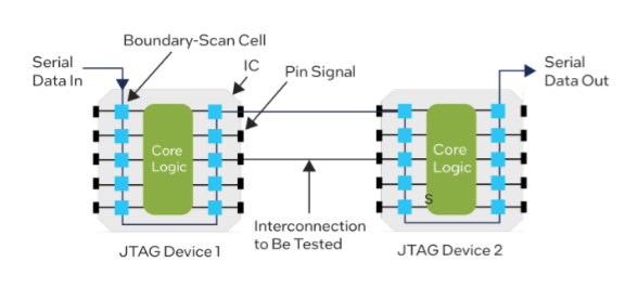
Figure 5: Boundary Scan
Similarly, use of machine learning classification algorithms and data analytics can identify patterns in the massive test output data, leading to more efficient testing strategies and faster defect detection.
Test engineers should run more critical tests first and lesser-critical tests later. If a chip fails the critical tests, then it precludes the need to run any further tests, thereby saving test time. Similarly, the tests that historically have enjoyed a very high success rate need not be performed on all the chips. Running these tests on a few chips sampled from a larger inventory should suffice for all practical purposes.
Some researchers have also proposed reducing the ATE test time by voltage and frequency scaling. By cranking up the operating voltage and increasing the test clock frequency, the test time can be significantly reduced. This can, however, be a double-edged sword. In addition to introducing hold time and setup time violations respectively, increasing voltage and frequency can also cause voltage droop or ground bounce to increase beyond the spec, and may introduce false failures during testing.
In the dynamic landscape or semiconductor manufacturing where innovation and efficiency are paramount, the optimization of test time stands as a pivotal endeavor. The impact of shortened test cycles extends far beyond the production floor, reaching into market responsiveness, cost-effectiveness, and overall product quality. By embracing strategies that reduce test times, manufactures can swiftly translate ideas into tangible products, meet evolving consumer demands with agility, and realize substantial cost savings.
References:


