

Get the semiconductor daily news directly to you by subscribing to our email list. For ASIC designer and managers, staying updated with the latest news, technologies, and trends is crucial. Here are the lastest news from the semiconductor industry.

While assembly houses are gradually becoming more and more organized in regards to following internal processes, it seems that we, their customers, are often trying to push them to make shortcuts only because “we are running out of time”.
With chip design cycle time shrinking, production related tasks such

This is a guest post by Naman Gupta, a Static Timing Analysis (STA) engineer at a leading semiconductor company in India.
Electrostatic Discharge and Electromigration might sound similar, but refer to two different physical phenomena. Let’s take them up one by one.
Electrostatic Discharge (ESD) is the large current flow between any
Each year, top foundries are ranked by their sales, and you probably don’t need the table below to know who’s first.
But what if we look at the top foundries from the capacity angle? Each of the top foundries holds several production lines that address different technology nodes and wafer

This is a guest post by Naman Gupta, a Static Timing Analysis (STA) engineer at a leading semiconductor company in India.
Lock-Up Latches are important elements for STA engineer while closing timing on their DFT Modes: particularly the hold timing closure of the Shift Mode. While shifting, the scan chains

Maskset cost is becoming one of the major expenses to the overall NRE cost of ASIC projects, particularly with advanced technology nodes. For projects targeting low volume production the maskset cost is a financial barrier to a profitable and solid business.
Taping out using MLM instead of a full maskset

Dr. Morris Chang is not my hero. He might be the most important person in the semiconductor industry in our lifetime, but he is not my hero. I have nothing against him. I’ve never met him and probably will never will. Instead, I meet my heroes usually after tape-out,

Simply defined, Latch-Up in VLSI is a functional chip failure associated with excessive current going through the chip, caused by weak circuit design. In some cases Latch-Up can be a temporary condition that can be resolved by power cycle, but unfortunately it can also cause a fatal chip failure.
Read More

How many ASIC service providers are typically included in a shortlist when launching a project?
We’d argue that too few.
There are over 2000 ASIC service providers worldwide that provide a range of services – ASIC design, verification, validation, packaging, testing, or supply chain solutions, which combine multiple services.
Semiconductor foundries claim they release a new technology node every two years. They may be off by a year or two, but on the whole, this is quite impressive, no doubt. Come to think of it, I don’t believe many of us even change our mobile phone every two years. How
Read More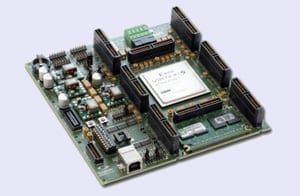
With the increased complexity of SoC designs, high tapeout prices and shrinking time-to-market, ASIC Prototyping has become a key step in ASIC projects. FPGA development boards are being used more often to verify ASIC design, test hardware and software integration, and provide a proof of concept demonstration to potential customers
Read More