
In this guide, we’ll elucidate the pivotal role of FO-PLP in advancing the semiconductor sector. Harnessing cost-effectiveness with enhanced functionality, FO-PLP beckons a new era of electronic sophistication. Let’s delve into the ultimate guide to Fan-Out Panel-Level Packaging and explore how it’s shaping the future.
Overview of Fan-Out Panel-Level

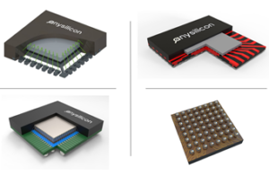
In this guide, we’ll delve into what exactly embedded die packaging is, exploring its definition, and the myriad of benefits it provides across various applications. From space-saving designs to improved heat dissipation, this innovative approach to integrating semiconductor dies is pivotal for modern electronics.
Image courtesy: ASE
Read More
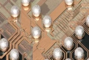
Introduction to Integrated Circuit Packaging
Integrated circuit packaging technologies have evolved throughout the years to the point where hundreds of IC package types are available today.
Most applications will require the more general, single-element packaging for integrated circuits and the other components such as resistors, capacitators, antenna etc.
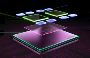
In order to cater to the computing demands for high performance computing (HPC) and artificial intelligence (AI), a need for a scalable package was felt. Chip-on-wafer-on-substrate (CoWoS) refers to the advanced packaging technology that offers the advantage of a larger package size and more I/O connections. It allows 2.5D and
Read More
iNPACK (a PCB Technologies Ltd. Company) and cutting-edge IC packaging and assembly house in Israel, in conjunction with ATS Engineering, a leading IC Test House based in Israel, have announced a transformative collaboration in order to establish the first Outsourced Semiconductor Assembly and Test (OSAT) facility in the Middle East. This pioneering venture aims to
Read More
Since mid of last year, our member ESPAT-Consulting is dedicating significant resources to SEMI Europe GmbH in Berlin, Germany, as one of the seven consortium core members of the EU CHIPS ACT driven Horizon Europe – Chips Joint Undertaking (JU) – Coordination and Support Action (CSA) – Project Pack4EU (Link: https://pack4eu.eu/). He is asking
Read More