

Get the semiconductor daily news directly to you by subscribing to our email list. For ASIC designer and managers, staying updated with the latest news, technologies, and trends is crucial. Here are the lastest news from the semiconductor industry.

Cesson-Sévigné (France) – June 29, 2023 – Secure-IC, the rising leader, and the unique global provider of end-to-end cybersecurity solutions for embedded systems and connected objects, announces today its SecuryzrTM successfully became ISO 26262 ASIL-D certified. This achievement highlights Secure-IC’s commitment to delivering the highest level of functional safety and
Read More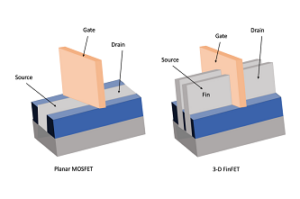
Introduction to FinFETs
In the quest for smaller, faster, and more power-efficient electronic devices, the evolution of semiconductor technology has been relentless. One significant milestone in this journey has been the advent of FinFETs (Fin Field-Effect Transistors). FinFETs have emerged as a ground-breaking transistor design that has revolutionized the

Artificial Intelligence (AI) and Machine Learning (ML) have emerged as transformative technologies, revolutionizing numerous industries across the globe. The realm of electronic design automation (EDA) has also been revolutionized by artificial intelligence and machine learning. EDA plays a crucial role in the modern world, as it is responsible for designing
Read More
Santa Clara, CA, – June 19, 2023 – MosChip Technologies, a semiconductor and system design services company, announced that Dr. Naveed Sherwani has been appointed as “Non-Executive Director” of the Company.
Dr. Sherwani has decades of experience in entrepreneurship, technical engineering and general management. Dr. Sherwani currently serves as Chairman,
Physical design engineers are responsible for creating integrated circuits (ICs) and SoCs by designing layouts. One of the important considerations in IC design is power consumption. Here are some tips for physical design engineers to save power:
Clock Gating
One of the most effective ways to reduce power

Cesson-Sévigné (France) and Tokyo (Japan) – June 15th, 2023 – Secure-IC, the rising leader, and the unique global provider of end-to-end cybersecurity solutions for embedded systems and connected objects, announces today their extended partnership with NSITEXE, Inc. NSITEXE is a wholly owned subsidiary of Denso Corporation that develops and sells high efficiency
Read More
ILPITAS, CALIFORNIA, UNITED STATES — June 14, 2023 — Signature IP, a leading IP startup renowned for its configurable and flexible NoC platforms, has partnered with IPro Silicon IP, a top sales outsourcing provider in Israel. This partnership aims to bring advanced NoC and Connectivity solutions to the SoC design community
Read More
MILPITAS, CALIFORNIA, UNITED STATES, June 4, 2023/EINPresswire.com/ — Marquee Semiconductor, a leading global provider of connectivity solutions for SoC/Chiplets and FPGAs, is pleased to announce the successful acquisition of Semikunn Technology Services, a prominent design services company based in India. This strategic move further strengthens Marquee Semiconductor’s position as a
Read More
OUTLINE
Semiconductor probe card revenues are down by 0.5% in 2022.
Reaching US$1.84 billion in 2022, revenue from sockets is on track to reach a record high.
Revenue from advanced PCBs grew overall in 2022, driven by sales of DIBs.
The Top 3 probe card suppliers
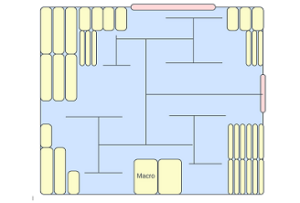
Floorplanning plays a crucial role in the physical design of an SoC and lays the foundation for an efficient and high-performance ASIC layout. In this article, we will discuss ten essential floorplanning commandments that physical design engineers can follow to ensure a correct-by-construction design.
Design Partitioning
Design Partitioning